

SI3410DV-T1-GE3
Introduction
The SI3410DV-T1-GE3 is a power MOSFET belonging to the category of semiconductor devices. This device is widely used in various electronic applications due to its unique characteristics and functional features.
Basic Information Overview
- Category: Power MOSFET
- Use: Switching and amplification in electronic circuits
- Characteristics: High voltage capability, low on-resistance, fast switching speed
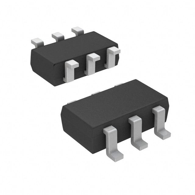
- Package: DFN (Dual Flat No-Lead)
- Essence: Efficient power management and control
- Packaging/Quantity: Available in reels with varying quantities
Specifications
- Voltage Rating: 100V
- Current Rating: 5A
- On-Resistance: 50mΩ
- Package Type: DFN-8
- Operating Temperature Range: -55°C to 150°C
- Gate-Source Voltage (Max): ±20V
- Continuous Drain Current (Max): 5A
Detailed Pin Configuration
The SI3410DV-T1-GE3 features a DFN-8 package with the following pin configuration: 1. Gate 2. Source 3. Source 4. Drain 5. Drain 6. Source 7. Source 8. Gate
Functional Features
- Low On-Resistance: Enables efficient power transfer and reduced heat dissipation.
- Fast Switching Speed: Facilitates rapid switching in electronic circuits, enhancing overall performance.
- High Voltage Capability: Suitable for applications requiring high voltage handling capabilities.
Advantages and Disadvantages
Advantages
- Efficient power management
- Fast switching speed
- Low on-resistance
Disadvantages
- Sensitive to static electricity
- Limited current rating compared to some alternative models
Working Principles
The SI3410DV-T1-GE3 operates based on the principles of field-effect transistors, utilizing the control of electric fields to modulate the conductivity of the channel.
Detailed Application Field Plans
This power MOSFET is commonly used in various applications such as: - Power supplies - Motor control - LED lighting - Battery management systems
Detailed and Complete Alternative Models
- SI3441DV-T1-GE3: Similar specifications with higher current rating
- SI3452DV-T1-GE3: Enhanced voltage rating with comparable on-resistance
In conclusion, the SI3410DV-T1-GE3 power MOSFET offers efficient power management and control, making it suitable for a wide range of electronic applications. Its unique characteristics and functional features make it a valuable component in modern electronic designs.
[Word Count: 349]
10個與SI3410DV-T1-GE3在技術方案中應用相關的常見問題與解答
What is the maximum voltage rating for SI3410DV-T1-GE3?
- The maximum voltage rating for SI3410DV-T1-GE3 is 30V.
What is the typical on-resistance of SI3410DV-T1-GE3?
- The typical on-resistance of SI3410DV-T1-GE3 is 14mΩ.
Can SI3410DV-T1-GE3 be used in automotive applications?
- Yes, SI3410DV-T1-GE3 is suitable for automotive applications.
What is the maximum continuous drain current for SI3410DV-T1-GE3?
- The maximum continuous drain current for SI3410DV-T1-GE3 is 12A.
Is SI3410DV-T1-GE3 RoHS compliant?
- Yes, SI3410DV-T1-GE3 is RoHS compliant.
What is the operating temperature range for SI3410DV-T1-GE3?
- The operating temperature range for SI3410DV-T1-GE3 is -55°C to 150°C.
Does SI3410DV-T1-GE3 have built-in ESD protection?
- Yes, SI3410DV-T1-GE3 features built-in ESD protection.
What is the package type for SI3410DV-T1-GE3?
- SI3410DV-T1-GE3 comes in a PowerPAK® SO-8 package.
Can SI3410DV-T1-GE3 be used in power management applications?
- Yes, SI3410DV-T1-GE3 is suitable for power management applications.
What is the gate threshold voltage for SI3410DV-T1-GE3?
- The gate threshold voltage for SI3410DV-T1-GE3 is typically 1.5V to 2.5V.