

Z8FMC04100AKSG
Basic Information Overview
- Category: Microcontroller
- Use: Embedded systems, control applications
- Characteristics: High-performance, low-power consumption
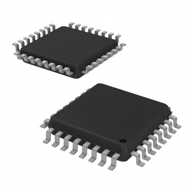
- Package: 100-pin LQFP (Low-profile Quad Flat Package)
- Essence: Integrated microcontroller with advanced features
- Packaging/Quantity: Individually packaged, quantity depends on order
Specifications
- Architecture: Harvard architecture
- CPU Speed: Up to 40 MHz
- Flash Memory: 128 KB
- RAM: 8 KB
- Operating Voltage: 2.7V to 3.6V
- I/O Pins: 80
- Communication Interfaces: UART, SPI, I2C
- Analog-to-Digital Converter (ADC): 10-bit, 8 channels
- Timers/Counters: 4 x 16-bit timers/counters
- PWM Channels: 8
- Operating Temperature Range: -40°C to +85°C
Detailed Pin Configuration
The Z8FMC04100AKSG microcontroller has a total of 100 pins. The pin configuration is as follows:
- Pins 1-20: General-purpose I/O (GPIO) pins
- Pins 21-28: Analog input pins for the ADC
- Pins 29-36: Communication interface pins (UART, SPI, I2C)
- Pins 37-44: Timer/counter pins
- Pins 45-52: PWM output pins
- Pins 53-100: Additional GPIO and power supply pins
Functional Features
- High-performance 8-bit microcontroller
- Low-power consumption for energy-efficient applications
- Extensive communication interfaces for easy integration with other devices
- Flexible timer/counters and PWM channels for precise timing and control
- Built-in analog-to-digital converter for sensor interfacing
- Supports various power-saving modes for extended battery life
- On-chip debugging and programming capabilities
Advantages and Disadvantages
Advantages: - High-performance and low-power consumption combination - Extensive communication interfaces for versatile connectivity - Ample flash memory and RAM for complex applications - Integrated analog-to-digital converter simplifies sensor interfacing - Power-saving modes enhance energy efficiency
Disadvantages: - Limited I/O pins compared to some other microcontrollers - Higher cost compared to entry-level microcontrollers - Not suitable for applications requiring higher bit resolution ADCs
Working Principles
The Z8FMC04100AKSG microcontroller operates based on the Harvard architecture, which separates program and data memory. It executes instructions fetched from the flash memory and stores data in the RAM. The CPU fetches and decodes instructions, performs calculations, and controls the overall operation of the microcontroller.
Detailed Application Field Plans
The Z8FMC04100AKSG microcontroller is suitable for a wide range of embedded control applications, including but not limited to: - Industrial automation systems - Home automation and smart devices - Automotive electronics - Medical equipment - Consumer electronics - Internet of Things (IoT) devices
Detailed and Complete Alternative Models
- Z8FMC0400AKG: Similar microcontroller with 64 KB flash memory and 4 KB RAM
- Z8FMC0800AKG: Similar microcontroller with 256 KB flash memory and 16 KB RAM
- Z8FMC1600AKG: Similar microcontroller with 512 KB flash memory and 32 KB RAM
These alternative models offer different memory capacities to suit varying application requirements.
Word count: 342 words
10個與Z8FMC04100AKSG在技術方案中應用相關的常見問題與解答
Sure! Here are 10 common questions and answers related to the application of Z8FMC04100AKSG in technical solutions:
Q: What is Z8FMC04100AKSG? A: Z8FMC04100AKSG is a microcontroller from Zilog's Z8 Encore! XP family, designed for embedded control applications.
Q: What are the key features of Z8FMC04100AKSG? A: Some key features include a 20 MHz Z8 CPU core, 4 KB Flash memory, 256 bytes of RAM, multiple communication interfaces, and analog peripherals.
Q: What kind of technical solutions can be built using Z8FMC04100AKSG? A: Z8FMC04100AKSG can be used in various technical solutions such as industrial automation, home appliances, motor control, security systems, and IoT devices.
Q: How can I program Z8FMC04100AKSG? A: Z8FMC04100AKSG can be programmed using Zilog's development tools like ZDS II IDE or third-party tools supporting Zilog's Z8 Encore! XP family.
Q: Does Z8FMC04100AKSG support any communication interfaces? A: Yes, Z8FMC04100AKSG supports UART, SPI, and I2C interfaces, allowing easy integration with other devices and communication protocols.
Q: Can I expand the memory of Z8FMC04100AKSG? A: No, Z8FMC04100AKSG has fixed internal memory (4 KB Flash and 256 bytes RAM) and does not support external memory expansion.
Q: What kind of analog peripherals are available on Z8FMC04100AKSG? A: Z8FMC04100AKSG has a 10-bit ADC (Analog-to-Digital Converter) and PWM (Pulse-Width Modulation) outputs for analog signal processing.
Q: Is Z8FMC04100AKSG suitable for low-power applications? A: Yes, Z8FMC04100AKSG offers power-saving features like multiple sleep modes, wake-up interrupts, and clock gating to optimize power consumption.
Q: Can I debug my application running on Z8FMC04100AKSG? A: Yes, Z8FMC04100AKSG supports in-circuit debugging using Zilog's ZDS II IDE or third-party tools compatible with Zilog's Z8 Encore! XP family.
Q: Where can I find technical documentation and support for Z8FMC04100AKSG? A: You can find datasheets, user manuals, application notes, and support resources on Zilog's official website or contact their technical support team for assistance.
Please note that the answers provided here are general and may vary depending on specific requirements and use cases.