

XC7VX485T-1FFG1761C
Product Overview
Category
The XC7VX485T-1FFG1761C belongs to the category of Field-Programmable Gate Arrays (FPGAs).
Use
FPGAs are integrated circuits that can be programmed after manufacturing. The XC7VX485T-1FFG1761C is specifically designed for high-performance applications, offering flexibility and reconfigurability.
Characteristics
- High-performance FPGA with advanced features
- Large capacity and high-speed processing capabilities
- Configurable logic blocks and programmable interconnects
- Support for various communication protocols
- Low power consumption
- Robust and reliable design
Package
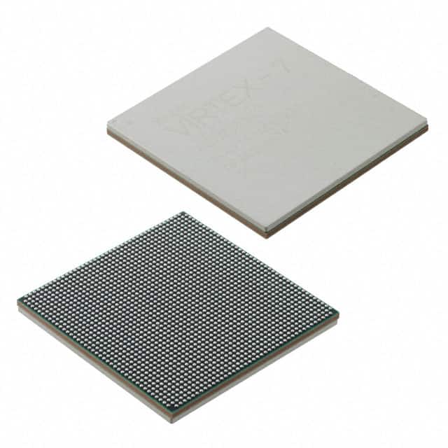
The XC7VX485T-1FFG1761C comes in a specific package known as the 1761-pin Flip-Chip Fine-Pitch Ball Grid Array (FFG1761C).
Essence
The essence of the XC7VX485T-1FFG1761C lies in its ability to provide a customizable hardware platform for implementing complex digital systems.
Packaging/Quantity
The XC7VX485T-1FFG1761C is typically packaged individually and is available in various quantities depending on the manufacturer's specifications.
Specifications
- Logic Cells: 485,760
- DSP Slices: 3,600
- Block RAM: 68,400 Kb
- Maximum I/O Pins: 1,761
- Operating Voltage: 1.0V
- Operating Temperature Range: -40°C to +100°C
- Package Dimensions: 45mm x 45mm
Detailed Pin Configuration
The XC7VX485T-1FFG1761C has a complex pin configuration with 1,761 pins. For detailed information on the pin assignments and their functions, please refer to the manufacturer's datasheet.
Functional Features
- High-speed data processing capabilities
- Configurable logic blocks for implementing custom digital circuits
- Support for various communication protocols (e.g., PCIe, Ethernet)
- On-chip memory resources for efficient data storage and retrieval
- Flexible I/O interfaces for seamless integration with external devices
- Advanced clock management features for precise timing control
Advantages and Disadvantages
Advantages
- Flexibility and reconfigurability for adapting to changing requirements
- High-performance computing capabilities
- Lower development time compared to custom ASIC designs
- Cost-effective solution for prototyping and low-volume production
Disadvantages
- Higher power consumption compared to dedicated hardware solutions
- Limited performance compared to application-specific integrated circuits (ASICs)
- Steeper learning curve for programming and utilizing FPGA features effectively
Working Principles
The XC7VX485T-1FFG1761C operates based on the principles of reconfigurable computing. It consists of configurable logic blocks interconnected through programmable routing resources. The user can program the FPGA to implement desired digital circuits by configuring the logic blocks and interconnects using a Hardware Description Language (HDL) or graphical tools provided by the manufacturer.
Detailed Application Field Plans
The XC7VX485T-1FFG1761C finds applications in various fields, including:
- Telecommunications: Used in high-speed data transmission systems, network routers, and switches.
- Aerospace and Defense: Employed in radar systems, avionics, and secure communication equipment.
- Industrial Automation: Utilized in control systems, robotics, and real-time monitoring devices.
- Medical Electronics: Applied in medical imaging, diagnostic equipment, and patient monitoring systems.
- Automotive: Integrated into advanced driver-assistance systems (ADAS), infotainment systems, and engine control units.
Detailed and Complete Alternative Models
- XC7VX690T-2FFG1761C: A higher-capacity FPGA with 690,720 logic cells and similar features.
- XC7VX980T-2FFG1761C: An even larger FPGA with 980,160 logic cells, suitable for complex applications.
- XC7VX1140T-2FFG1761C: A high-performance FPGA with 1,140,480 logic cells, offering enhanced processing capabilities.
These alternative models provide increased capacity and performance options for users with more demanding requirements.
In conclusion, the XC7VX485T-1FFG1761C is a high-performance FPGA that offers flexibility, reconfigurability, and advanced features. It finds applications in various fields and provides a customizable hardware platform for implementing complex digital systems. While it has advantages such as adaptability and cost-effectiveness, it also has limitations in terms of power consumption and performance compared to ASICs. Nonetheless, the XC7VX485T-1FFG1761C remains a valuable tool for designers seeking
10個與XC7VX485T-1FFG1761C在技術方案中應用相關的常見問題與解答
Sure! Here are 10 common questions and answers related to the application of XC7VX485T-1FFG1761C in technical solutions:
Q1: What is XC7VX485T-1FFG1761C? A1: XC7VX485T-1FFG1761C is a specific model of Xilinx Virtex-7 FPGA (Field-Programmable Gate Array) that offers high-performance processing capabilities for various technical applications.
Q2: What are the key features of XC7VX485T-1FFG1761C? A2: Some key features of XC7VX485T-1FFG1761C include a large number of programmable logic cells, high-speed serial transceivers, embedded memory blocks, DSP slices, and support for various communication protocols.
Q3: What are the typical applications of XC7VX485T-1FFG1761C? A3: XC7VX485T-1FFG1761C is commonly used in applications such as high-performance computing, aerospace and defense systems, telecommunications, video processing, medical imaging, and scientific research.
Q4: How can XC7VX485T-1FFG1761C be programmed? A4: XC7VX485T-1FFG1761C can be programmed using Xilinx's Vivado Design Suite, which provides a comprehensive set of tools for designing, implementing, and debugging FPGA-based solutions.
Q5: What is the power consumption of XC7VX485T-1FFG1761C? A5: The power consumption of XC7VX485T-1FFG1761C depends on the specific configuration and operating conditions. It is recommended to refer to the datasheet or consult Xilinx's documentation for detailed power consumption information.
Q6: Can XC7VX485T-1FFG1761C be used in safety-critical applications? A6: Yes, XC7VX485T-1FFG1761C can be used in safety-critical applications. However, it is important to follow industry best practices and perform thorough verification and validation processes to ensure the reliability and safety of the overall system.
Q7: Does XC7VX485T-1FFG1761C support high-speed serial communication? A7: Yes, XC7VX485T-1FFG1761C supports high-speed serial communication through its built-in transceivers, which can be configured to support various protocols such as PCIe, SATA, Ethernet, and more.
Q8: Can XC7VX485T-1FFG1761C interface with external memory devices? A8: Yes, XC7VX485T-1FFG1761C has embedded memory blocks and also supports interfacing with external memory devices such as DDR3/DDR4 SDRAM, QDR SRAM, Flash memory, and more.
Q9: What development boards or evaluation kits are available for XC7VX485T-1FFG1761C? A9: Xilinx offers various development boards and evaluation kits that feature XC7VX485T-1FFG1761C, such as the VC707 Evaluation Kit and the KC705 Evaluation Kit. These kits provide a platform for prototyping and testing designs based on this FPGA.
Q10: Are there any specific design considerations when using XC7VX485T-1FFG1761C? A10: Yes, when designing with XC7VX485T-1FFG1761C, it is important to consider factors such as power supply requirements, thermal management, signal integrity, and timing constraints to ensure optimal performance and reliability of the system.
Please note that these answers are general and may vary depending on specific design requirements and application scenarios. It is always recommended to consult the official documentation and resources provided by Xilinx for accurate and up-to-date information.