

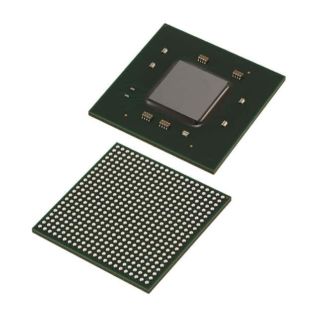
XC7K160T-1FB484I
Product Overview
Category
The XC7K160T-1FB484I belongs to the category of Field Programmable Gate Arrays (FPGAs).
Use
FPGAs are integrated circuits that can be programmed and reprogrammed to perform various functions. The XC7K160T-1FB484I is specifically designed for high-performance applications that require complex digital logic and signal processing.
Characteristics
- High-performance FPGA with advanced features
- Large capacity and high-speed processing capabilities
- Flexible and customizable design options
- Suitable for a wide range of applications
Package
The XC7K160T-1FB484I comes in a FB484 package, which refers to the type of chip packaging used. This package provides a compact and efficient form factor for easy integration into electronic systems.
Essence
The essence of the XC7K160T-1FB484I lies in its ability to provide a programmable hardware platform that enables designers to implement complex digital systems with high performance and flexibility.
Packaging/Quantity
The XC7K160T-1FB484I is typically sold individually or in small quantities, depending on the supplier and customer requirements.
Specifications
- FPGA Family: Kintex-7
- Logic Cells: 159,200
- DSP Slices: 480
- Block RAM: 4,860 Kb
- Maximum Frequency: 400 MHz
- I/O Pins: 484
- Operating Voltage: 1.0V
Detailed Pin Configuration
The XC7K160T-1FB484I has a total of 484 I/O pins, each serving a specific purpose in the system design. The pin configuration varies depending on the specific application and user requirements. For detailed pin assignments and configurations, please refer to the manufacturer's documentation.
Functional Features
The XC7K160T-1FB484I offers several functional features that make it a versatile FPGA for various applications:
- High-performance processing capabilities
- Flexible and customizable design options
- Support for advanced digital signal processing algorithms
- Integrated memory blocks for efficient data storage
- Multiple I/O interfaces for seamless integration with external devices
Advantages and Disadvantages
Advantages
- High processing power and performance
- Flexibility in design and customization
- Support for complex digital systems
- Efficient use of resources
- Wide range of available tools and support
Disadvantages
- Steep learning curve for beginners
- Higher cost compared to other programmable logic devices
- Requires expertise in FPGA programming and design
Working Principles
The XC7K160T-1FB484I operates based on the principles of reconfigurable hardware. It consists of a matrix of configurable logic blocks interconnected through programmable routing resources. The user can program the FPGA using Hardware Description Languages (HDL) such as VHDL or Verilog, defining the desired functionality and interconnections.
Once programmed, the FPGA executes the specified logic operations, enabling the implementation of complex digital systems. The ability to reprogram the FPGA allows for iterative design improvements and adaptability to changing requirements.
Detailed Application Field Plans
The XC7K160T-1FB484I finds applications in various fields, including:
- Communications: Used in wireless base stations, network routers, and high-speed data transmission systems.
- Aerospace and Defense: Employed in radar systems, avionics, and secure communication systems.
- Industrial Automation: Utilized in control systems, robotics, and machine vision applications.
- Medical Devices: Integrated into medical imaging equipment, patient monitoring systems, and diagnostic instruments.
- Automotive: Applied in advanced driver assistance systems (ADAS), infotainment systems, and engine control units.
Detailed and Complete Alternative Models
- XC7K325T-1FFG900C: A higher-capacity FPGA from the same Kintex-7 family, offering 324,000 logic cells and 900 I/O pins.
- XC7A100T-1CSG324I: An alternative FPGA from the Artix-7 family, providing a lower-cost option with 101,440 logic cells and 324 I/O pins.
- XC7Z020-1CLG484I: A hybrid FPGA and ARM processor from the Zynq-7000 family, combining programmable logic with dual-core ARM Cortex-A9 processors.
These alternative models offer different capacities, pin counts, and features to suit specific application requirements.
Word count: 550 words
10個與XC7K160T-1FB484I在技術方案中應用相關的常見問題與解答
Sure! Here are 10 common questions and answers related to the application of XC7K160T-1FB484I in technical solutions:
Q1: What is XC7K160T-1FB484I? A1: XC7K160T-1FB484I is a specific model of Xilinx's Kintex-7 FPGA (Field Programmable Gate Array) family. It offers 160,000 logic cells and is packaged in a FB484 package.
Q2: What are the key features of XC7K160T-1FB484I? A2: Some key features of XC7K160T-1FB484I include high-performance programmable logic, integrated memory blocks, DSP slices for signal processing, and multiple I/O standards.
Q3: What are the typical applications of XC7K160T-1FB484I? A3: XC7K160T-1FB484I is commonly used in various technical solutions such as wireless communication systems, industrial automation, video processing, medical imaging, and aerospace applications.
Q4: How can XC7K160T-1FB484I be programmed? A4: XC7K160T-1FB484I can be programmed using Xilinx's Vivado Design Suite, which provides a comprehensive development environment for FPGA designs.
Q5: What are the power requirements for XC7K160T-1FB484I? A5: The power requirements for XC7K160T-1FB484I depend on the specific design and usage scenario. It typically requires a supply voltage of 0.95V for core logic and 1.8V for I/O banks.
Q6: Can XC7K160T-1FB484I be used in safety-critical applications? A6: Yes, XC7K160T-1FB484I can be used in safety-critical applications. However, additional measures such as redundancy and fault-tolerant design techniques may be required to ensure the desired level of reliability.
Q7: What is the maximum operating frequency of XC7K160T-1FB484I? A7: The maximum operating frequency of XC7K160T-1FB484I depends on the specific design and implementation. It can typically achieve frequencies in the range of several hundred megahertz to a few gigahertz.
Q8: Can XC7K160T-1FB484I interface with external devices? A8: Yes, XC7K160T-1FB484I supports various I/O standards and can interface with external devices such as memories, sensors, communication interfaces, and other peripherals.
Q9: Are there any development boards available for XC7K160T-1FB484I? A9: Yes, Xilinx offers development boards specifically designed for XC7K160T-1FB484I, such as the Kintex-7 KC705 Evaluation Kit, which provides a platform for prototyping and testing designs.
Q10: Can XC7K160T-1FB484I be used in low-power applications? A10: While XC7K160T-1FB484I is not specifically optimized for low-power applications, power-saving techniques such as clock gating, power management IP cores, and careful design practices can be employed to reduce power consumption.
Please note that these answers are general and may vary depending on the specific requirements and context of your technical solution.