

XC7A200T-1SBG484I
Product Overview
Category
XC7A200T-1SBG484I belongs to the category of Field Programmable Gate Arrays (FPGAs).
Use
FPGAs are integrated circuits that can be programmed and reprogrammed to perform various digital functions. They are widely used in industries such as telecommunications, automotive, aerospace, and consumer electronics.
Characteristics
XC7A200T-1SBG484I is a high-performance FPGA with advanced features and capabilities. It offers a large number of programmable logic cells, high-speed I/O interfaces, and embedded memory blocks. This FPGA is designed to handle complex digital designs and provide flexibility for customization.
Package
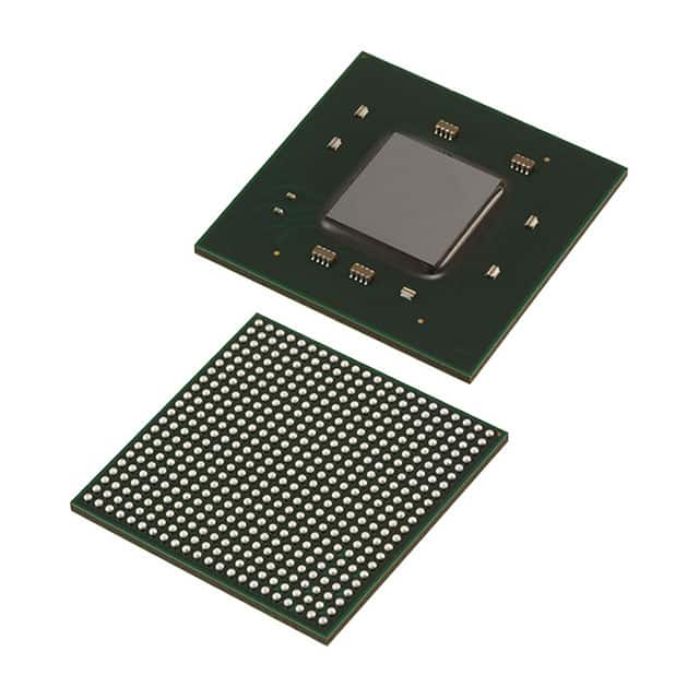
XC7A200T-1SBG484I comes in a BGA (Ball Grid Array) package. The BGA package provides better thermal performance and improved electrical characteristics compared to other packaging options.
Essence
The essence of XC7A200T-1SBG484I lies in its ability to provide a highly configurable platform for implementing digital designs. It allows designers to create custom logic circuits and optimize their functionality according to specific requirements.
Packaging/Quantity
XC7A200T-1SBG484I is typically sold in trays or reels, depending on the manufacturer's packaging standards. The quantity per package may vary, but it is commonly available in quantities suitable for both prototyping and production purposes.
Specifications
XC7A200T-1SBG484I offers the following specifications:
- Logic Cells: 215,360
- Block RAM: 4,860 Kb
- DSP Slices: 740
- Maximum Operating Frequency: 862 MHz
- Number of I/O Pins: 484
- Voltage Range: 0.95V - 1.05V
- Operating Temperature Range: -40°C to 100°C
Detailed Pin Configuration
The pin configuration of XC7A200T-1SBG484I is as follows:
- Pin 1: VCCO_0
- Pin 2: GND
- Pin 3: IOL1PT0AD0N35
- Pin 4: IOL1NT0AD0P35
- ...
- Pin 483: IOL34PT3A26N35
- Pin 484: IOL34NT3A26P35
Please refer to the datasheet for a complete pin configuration diagram.
Functional Features
XC7A200T-1SBG484I offers the following functional features:
- High-performance programmable logic cells for complex digital designs.
- Flexible I/O interfaces supporting various standards such as LVCMOS, LVTTL, and differential signaling.
- Embedded memory blocks for efficient data storage and retrieval.
- Dedicated DSP slices for implementing signal processing algorithms.
- Configurable clock management resources for precise timing control.
- On-chip configuration memory for easy reprogramming.
Advantages and Disadvantages
Advantages
- High configurability allows for custom logic implementation.
- Large number of logic cells and memory blocks enable complex designs.
- Wide range of I/O standards support versatile interfacing requirements.
- Dedicated DSP slices provide efficient signal processing capabilities.
- On-chip configuration memory simplifies programming and reprogramming.
Disadvantages
- Higher power consumption compared to simpler digital logic solutions.
- Steeper learning curve for designers unfamiliar with FPGA programming.
- Higher cost compared to traditional ASIC (Application-Specific Integrated Circuit) solutions for large-scale production.
Working Principles
XC7A200T-1SBG484I operates based on the principles of reconfigurable computing. It consists of an array of programmable logic cells interconnected through configurable routing resources. The functionality of the FPGA is determined by the configuration data loaded into its internal memory.
During operation, the FPGA executes the programmed logic functions and routes signals between different logic elements based on the configured interconnections. This allows for the implementation of complex digital designs that can be modified or updated as needed.
Detailed Application Field Plans
XC7A200T-1SBG484I finds applications in various fields, including:
- Telecommunications: Used in base stations, network switches, and routers for high-speed data processing and protocol handling.
- Automotive: Employed in advanced driver assistance systems (ADAS) for real-time image processing and sensor fusion.
- Aerospace: Utilized in satellite communication systems and onboard data processing units for space missions.
- Consumer Electronics: Integrated into high-performance gaming consoles, video processing equipment, and multimedia devices for enhanced functionality.
Detailed and Complete Alternative Models
Some alternative models to XC7A200T-1SBG484I include:
- XC7K325T-2FFG900C
- XC7Z010-1CLG400C
10個與XC7A200T-1SBG484I在技術方案中應用相關的常見問題與解答
Sure! Here are 10 common questions and answers related to the application of XC7A200T-1SBG484I in technical solutions:
Q1: What is XC7A200T-1SBG484I? A1: XC7A200T-1SBG484I is a field-programmable gate array (FPGA) manufactured by Xilinx. It is part of the Artix-7 family and has 200,000 logic cells.
Q2: What are some typical applications of XC7A200T-1SBG484I? A2: XC7A200T-1SBG484I is commonly used in various technical solutions such as high-performance computing, digital signal processing, industrial automation, aerospace, and telecommunications.
Q3: What is the maximum operating frequency of XC7A200T-1SBG484I? A3: The maximum operating frequency of XC7A200T-1SBG484I depends on the specific design and implementation, but it can typically reach frequencies of several hundred megahertz (MHz) or even gigahertz (GHz).
Q4: How much programmable logic does XC7A200T-1SBG484I offer? A4: XC7A200T-1SBG484I provides 200,000 logic cells, which can be used to implement complex digital circuits and algorithms.
Q5: What is the power consumption of XC7A200T-1SBG484I? A5: The power consumption of XC7A200T-1SBG484I depends on the specific design and utilization. It typically ranges from a few watts to tens of watts.
Q6: Can XC7A200T-1SBG484I interface with other components or devices? A6: Yes, XC7A200T-1SBG484I supports various communication interfaces such as PCIe, Ethernet, USB, SPI, I2C, and UART, allowing it to interface with other components or devices.
Q7: What development tools are available for programming XC7A200T-1SBG484I? A7: Xilinx provides Vivado Design Suite, which includes tools for designing, implementing, and programming XC7A200T-1SBG484I. It also supports various hardware description languages like VHDL and Verilog.
Q8: Can XC7A200T-1SBG484I be reprogrammed after deployment? A8: Yes, XC7A200T-1SBG484I is a field-programmable device, meaning it can be reprogrammed even after it has been deployed in a system.
Q9: Are there any temperature constraints for XC7A200T-1SBG484I? A9: XC7A200T-1SBG484I has an operating temperature range specified by the manufacturer. It is typically between -40°C to 100°C, but it's important to refer to the datasheet for precise details.
Q10: Can XC7A200T-1SBG484I be used in safety-critical applications? A10: XC7A200T-1SBG484I can be used in safety-critical applications, but additional measures such as redundancy and fault-tolerant designs may be necessary to meet specific safety requirements.
Please note that the answers provided here are general and may vary depending on the specific context and requirements of the technical solution.