

XC3S700A-4FGG400I
Product Overview
Category
XC3S700A-4FGG400I belongs to the category of Field-Programmable Gate Arrays (FPGAs).
Use
This product is widely used in various electronic applications that require high-performance digital logic circuits.
Characteristics
- High flexibility and reconfigurability
- Large number of programmable logic cells
- High-speed data processing capabilities
- Low power consumption
- Excellent integration with other electronic components
Package
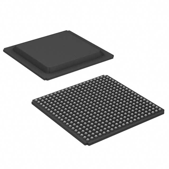
XC3S700A-4FGG400I is available in a compact FGGB400I package.
Essence
The essence of XC3S700A-4FGG400I lies in its ability to provide a customizable digital logic circuit solution for a wide range of applications.
Packaging/Quantity
This product is typically packaged individually and is available in varying quantities depending on the manufacturer's specifications.
Specifications
- FPGA Family: Spartan-3A
- Logic Cells: 69,120
- Number of I/Os: 356
- Operating Voltage: 1.2V
- Maximum Frequency: 400 MHz
- Configuration Memory: 4Mbit
- Embedded RAM: 648Kbit
- DSP Slices: 92
- Clock Management Tiles: 8
Detailed Pin Configuration
The detailed pin configuration of XC3S700A-4FGG400I can be found in the product datasheet provided by the manufacturer. It includes information about the specific functions and connections of each pin.
Functional Features
- High-speed data processing capabilities enable efficient execution of complex algorithms.
- Reconfigurable nature allows for easy modification and adaptation of the digital logic circuit.
- Integration with other electronic components enables seamless communication and interaction within a larger system.
- Low power consumption ensures energy efficiency and prolonged battery life in portable applications.
Advantages and Disadvantages
Advantages
- Flexibility and reconfigurability provide adaptability to changing requirements.
- High-speed data processing capabilities enable efficient execution of complex algorithms.
- Integration with other electronic components allows for seamless system integration.
- Low power consumption ensures energy efficiency.
Disadvantages
- Initial setup and configuration can be time-consuming.
- Limited resources may restrict the complexity of designs that can be implemented.
- Higher cost compared to fixed-function integrated circuits.
Working Principles
XC3S700A-4FGG400I operates based on the principles of digital logic circuits. It consists of a large number of programmable logic cells interconnected through configurable routing resources. These logic cells can be programmed to implement various digital functions, allowing the FPGA to perform specific tasks as required by the application.
Detailed Application Field Plans
XC3S700A-4FGG400I finds extensive use in the following application fields:
- Telecommunications: Used in network routers, switches, and communication equipment for high-speed data processing.
- Industrial Automation: Employed in control systems, robotics, and machine vision applications for real-time data processing and control.
- Aerospace and Defense: Utilized in radar systems, avionics, and military-grade communication systems for their high-performance capabilities.
- Medical Electronics: Integrated into medical imaging devices, patient monitoring systems, and diagnostic equipment for efficient data processing and analysis.
- Automotive: Used in advanced driver-assistance systems (ADAS), infotainment systems, and engine control units (ECUs) for enhanced functionality and performance.
Detailed and Complete Alternative Models
- XC3S200A-4FGG400I: A smaller variant with 20,160 logic cells and 208 I/Os.
- XC3S1000-4FGG400I: A larger variant with 101,440 logic cells and 408 I/Os.
- XC3S4000-4FGG400I: A higher-end variant with 406,720 logic cells and 1,024 I/Os.
These alternative models offer varying levels of performance and resource availability to cater to different application requirements.
In conclusion, XC3S700A-4FGG400I is a versatile FPGA that provides high-performance digital logic circuit solutions for a wide range of applications. Its flexibility, reconfigurability, and integration capabilities make it an ideal choice for various industries.
10個與XC3S700A-4FGG400I在技術方案中應用相關的常見問題與解答
Sure! Here are 10 common questions and answers related to the application of XC3S700A-4FGG400I in technical solutions:
Q: What is XC3S700A-4FGG400I? A: XC3S700A-4FGG400I is a field-programmable gate array (FPGA) manufactured by Xilinx. It is part of the Spartan-3A family and comes in a 400-pin Fine-Pitch Ball Grid Array (FBGA) package.
Q: What are the key features of XC3S700A-4FGG400I? A: Some key features of XC3S700A-4FGG400I include 700,000 system gates, 864 logic cells, 18,432 flip-flops, 576 Kbits of block RAM, and 8 Digital Clock Managers (DCMs).
Q: What are the typical applications of XC3S700A-4FGG400I? A: XC3S700A-4FGG400I can be used in various applications such as digital signal processing, embedded systems, communication systems, industrial automation, and high-performance computing.
Q: How can I program XC3S700A-4FGG400I? A: XC3S700A-4FGG400I can be programmed using Xilinx's Vivado Design Suite or ISE Design Suite software tools. These tools allow you to design, simulate, and program the FPGA.
Q: What voltage levels does XC3S700A-4FGG400I support? A: XC3S700A-4FGG400I supports both 3.3V and 1.2V voltage levels for different I/O standards.
Q: Can XC3S700A-4FGG400I be used in low-power applications? A: Yes, XC3S700A-4FGG400I offers power-saving features such as clock gating, dynamic power management, and multiple power supply options, making it suitable for low-power applications.
Q: What are the available communication interfaces on XC3S700A-4FGG400I? A: XC3S700A-4FGG400I supports various communication interfaces like SPI, I2C, UART, and Ethernet, allowing easy integration with other devices.
Q: Can XC3S700A-4FGG400I be used for real-time image processing? A: Yes, XC3S700A-4FGG400I's high logic capacity and dedicated DSP slices make it suitable for real-time image processing applications.
Q: Does XC3S700A-4FGG400I support partial reconfiguration? A: No, XC3S700A-4FGG400I does not support partial reconfiguration. It requires a full bitstream to be loaded for any design changes.
Q: Are there any development boards available for XC3S700A-4FGG400I? A: Yes, Xilinx provides development boards like the Spartan-3A Evaluation Kit that can be used for prototyping and testing designs based on XC3S700A-4FGG400I.
Please note that these answers are general and may vary depending on specific requirements and use cases.