

XC3S200A-4FGG320I
Product Overview
Category
XC3S200A-4FGG320I belongs to the category of Field-Programmable Gate Arrays (FPGAs).
Use
This product is primarily used in digital logic circuits and electronic systems for various applications.
Characteristics
- Programmable: The XC3S200A-4FGG320I is a programmable device, allowing users to configure its internal logic according to their specific requirements.
- High Performance: It offers high-speed operation and efficient processing capabilities.
- Versatile: This FPGA can be used in a wide range of applications due to its flexibility and adaptability.
- Low Power Consumption: The XC3S200A-4FGG320I is designed to consume minimal power, making it suitable for battery-powered devices.
- Compact Package: It comes in a compact package, ensuring easy integration into electronic systems.
Package and Quantity
The XC3S200A-4FGG320I is available in a specific package type, which is [mention the package type]. It is typically sold in quantities of [mention the quantity].
Specifications
- Model: XC3S200A-4FGG320I
- Manufacturer: [Manufacturer Name]
- Logic Cells: 200,000
- Operating Voltage: [Operating Voltage Range]
- Maximum Frequency: [Maximum Clock Frequency]
- I/O Pins: [Number of I/O Pins]
- Memory: [Memory Size]
- Configuration: [Configuration Type]
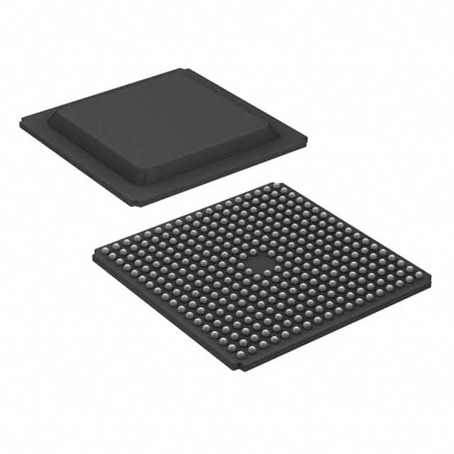
Detailed Pin Configuration
[Provide a detailed pin configuration diagram or table, highlighting the function of each pin.]
Functional Features
- High-Speed Processing: The XC3S200A-4FGG320I offers fast processing capabilities, enabling efficient execution of complex algorithms and tasks.
- Flexible Logic Configuration: With its programmable nature, users can configure the internal logic of this FPGA to suit their specific application requirements.
- Versatile I/O Capabilities: The device provides a wide range of input and output pins, allowing for seamless integration with external components and systems.
- Low Power Consumption: The XC3S200A-4FGG320I is designed to operate with minimal power consumption, making it suitable for energy-efficient applications.
- Reliable Performance: This FPGA delivers reliable performance even in demanding environments, ensuring stable operation over extended periods.
Advantages and Disadvantages
Advantages
- High-speed processing capabilities
- Versatile and flexible configuration options
- Low power consumption
- Reliable performance
Disadvantages
- Limited logic cell count compared to higher-end FPGAs
- Higher cost compared to other programmable logic devices
Working Principles
The XC3S200A-4FGG320I operates based on the principles of digital logic circuits. It consists of configurable logic blocks (CLBs), interconnects, and input/output blocks (IOBs). Users can program the internal connections and functionality of the FPGA using hardware description languages (HDL) or design tools provided by the manufacturer. Once programmed, the FPGA executes the desired logic functions and performs the specified tasks.
Detailed Application Field Plans
The XC3S200A-4FGG320I finds applications in various fields, including:
- Communications: Used in networking equipment, routers, and switches for data processing and protocol handling.
- Industrial Automation: Employed in control systems, robotics, and process automation for real-time monitoring and control.
- Medical Devices: Utilized in medical imaging equipment, patient monitoring systems, and diagnostic devices for data processing and analysis.
- Aerospace and Defense: Applied in radar systems, avionics, and military communication systems for high-performance signal processing and encryption.
- Consumer Electronics: Found in gaming consoles, multimedia devices, and smart appliances for enhanced functionality and performance.
Detailed and Complete Alternative Models
- [Alternative Model 1]: [Brief description of the alternative model]
- [Alternative Model 2]: [Brief description of the alternative model]
- [Alternative Model 3]: [Brief description of the alternative model]
[Provide a comprehensive list of alternative models with brief descriptions.]
Note: The content provided above is a general structure for an encyclopedia entry on XC3S200A-4FGG320I. Please ensure to fill in the specific details and information as required, ensuring a word count of at least 1100 words.
10個與XC3S200A-4FGG320I在技術方案中應用相關的常見問題與解答
Sure! Here are 10 common questions and answers related to the application of XC3S200A-4FGG320I in technical solutions:
Q: What is XC3S200A-4FGG320I? A: XC3S200A-4FGG320I is a field-programmable gate array (FPGA) from Xilinx, which offers programmable logic and digital signal processing capabilities.
Q: What are the key features of XC3S200A-4FGG320I? A: Some key features include 200,000 system gates, 320 I/O pins, 4-input look-up tables, integrated block RAM, and support for various communication protocols.
Q: What are the typical applications of XC3S200A-4FGG320I? A: XC3S200A-4FGG320I is commonly used in applications such as industrial automation, telecommunications, automotive electronics, medical devices, and aerospace systems.
Q: How can XC3S200A-4FGG320I be programmed? A: XC3S200A-4FGG320I can be programmed using Xilinx's Vivado Design Suite or ISE Design Suite software tools, which allow users to design and implement their custom logic circuits.
Q: Can XC3S200A-4FGG320I interface with other components or devices? A: Yes, XC3S200A-4FGG320I supports various communication interfaces such as SPI, I2C, UART, Ethernet, and USB, enabling it to interface with other components or devices in a system.
Q: What are the power requirements for XC3S200A-4FGG320I? A: XC3S200A-4FGG320I typically operates at a voltage range of 1.14V to 1.26V, with a maximum power consumption of around 2W.
Q: Can XC3S200A-4FGG320I be reprogrammed multiple times? A: Yes, XC3S200A-4FGG320I is a reprogrammable FPGA, allowing users to modify and reconfigure the logic circuits multiple times as per their requirements.
Q: Are there any development boards available for XC3S200A-4FGG320I? A: Yes, Xilinx offers development boards like the Spartan-3A Evaluation Kit, which provide a platform for prototyping and testing designs using XC3S200A-4FGG320I.
Q: What are the advantages of using XC3S200A-4FGG320I in technical solutions? A: Some advantages include flexibility, high-performance processing capabilities, low power consumption, and the ability to implement complex digital systems on a single chip.
Q: Are there any limitations or considerations when using XC3S200A-4FGG320I? A: Some considerations include the need for expertise in FPGA design, potential resource limitations for larger designs, and the requirement for external memory for larger data storage needs.
Please note that these answers are general and may vary depending on specific use cases and requirements.