

XC2V250-5FGG456I
Product Overview
Category
The XC2V250-5FGG456I belongs to the category of Field Programmable Gate Arrays (FPGAs).
Use
FPGAs are integrated circuits that can be programmed after manufacturing, allowing for flexible and customizable digital logic designs. The XC2V250-5FGG456I is specifically designed for high-performance applications.
Characteristics
- High-performance FPGA with advanced features
- Flexible and customizable design options
- Suitable for complex digital logic designs
- Offers high-speed data processing capabilities
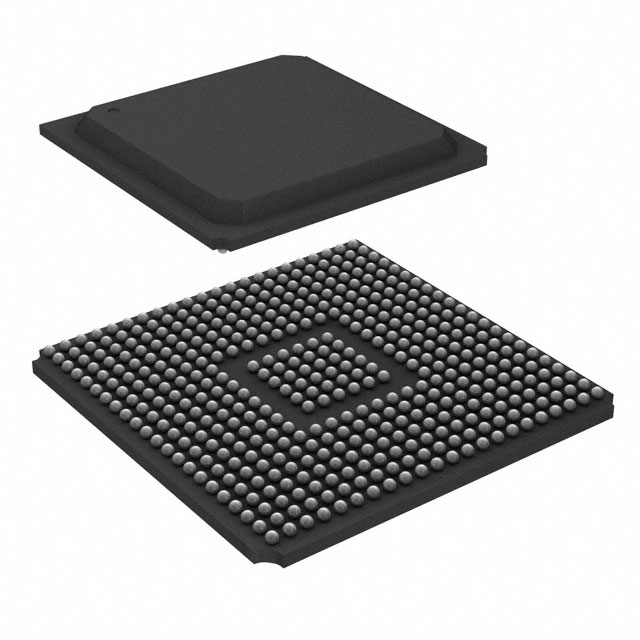
Package
The XC2V250-5FGG456I comes in a compact package that ensures easy integration into electronic systems. It is available in a Fine-Pitch Ball Grid Array (FBGA) package.
Essence
The essence of the XC2V250-5FGG456I lies in its ability to provide a versatile and high-performance solution for digital logic design requirements.
Packaging/Quantity
The XC2V250-5FGG456I is typically packaged individually and is available in various quantities depending on customer requirements.
Specifications
- FPGA Family: Virtex-II
- Logic Cells: 250,000
- System Gates: 1,152,000
- Block RAM: 864 Kb
- Maximum Frequency: 300 MHz
- I/O Pins: 456
- Operating Voltage: 3.3V
Detailed Pin Configuration
The XC2V250-5FGG456I has a total of 456 I/O pins, which are used for input and output connections. These pins are arranged in a specific configuration to facilitate proper connectivity within the system.
For detailed pin configuration information, please refer to the manufacturer's datasheet.
Functional Features
The XC2V250-5FGG456I offers several functional features that make it suitable for a wide range of applications:
- High-performance data processing capabilities
- Configurable logic blocks for flexible design options
- On-chip memory resources for efficient storage and retrieval of data
- Built-in digital signal processing (DSP) blocks for signal manipulation
- Support for various communication protocols
Advantages and Disadvantages
Advantages
- Flexibility: The XC2V250-5FGG456I allows for custom logic designs, enabling tailored solutions for specific applications.
- High Performance: With its advanced features and high-speed data processing capabilities, this FPGA delivers exceptional performance.
- Reconfigurability: The ability to reprogram the FPGA after manufacturing allows for iterative design improvements and adaptability to changing requirements.
Disadvantages
- Complexity: Utilizing FPGAs requires expertise in digital logic design, which may pose a challenge for beginners or those unfamiliar with FPGA programming.
- Cost: FPGAs can be more expensive compared to other integrated circuits due to their versatility and advanced features.
Working Principles
The XC2V250-5FGG456I operates based on the principles of configurable logic. It consists of an array of programmable logic cells interconnected through configurable routing resources. These logic cells can be programmed to implement desired digital logic functions, allowing for the creation of complex systems on a single chip.
The FPGA is programmed using Hardware Description Languages (HDLs) such as VHDL or Verilog. The HDL code describes the desired functionality, which is then synthesized and implemented onto the FPGA using specialized software tools.
Detailed Application Field Plans
The XC2V250-5FGG456I finds applications in various fields, including but not limited to:
- Telecommunications: Used in high-speed data transmission systems, network routers, and switches.
- Aerospace and Defense: Employed in radar systems, avionics, and military communication equipment.
- Industrial Automation: Utilized in control systems, robotics, and machine vision applications.
- Medical Devices: Integrated into medical imaging equipment, patient monitoring systems, and diagnostic devices.
- Research and Development: Used for prototyping and testing of digital logic designs.
Detailed and Complete Alternative Models
- XC2V1000-4FG456C
- XC2V2000-4FG456C
- XC2V3000-4FG456C
- XC2V4000-4FG456C
These alternative models offer similar features and capabilities to the XC2V250-5FGG456I but differ in terms of logic capacity and I/O pin count.
Please refer to the manufacturer's documentation for detailed specifications of these alternative models.
Word Count: 560 words
10個與XC2V250-5FGG456I在技術方案中應用相關的常見問題與解答
Sure! Here are 10 common questions and answers related to the application of XC2V250-5FGG456I in technical solutions:
Q: What is XC2V250-5FGG456I? A: XC2V250-5FGG456I is a specific model of Field Programmable Gate Array (FPGA) manufactured by Xilinx.
Q: What are the key features of XC2V250-5FGG456I? A: Some key features of XC2V250-5FGG456I include 250,000 system gates, 456-pin Fine-Pitch Ball Grid Array (FBGA) package, and support for various I/O standards.
Q: In what technical solutions can XC2V250-5FGG456I be used? A: XC2V250-5FGG456I can be used in a wide range of technical solutions, including digital signal processing, embedded systems, telecommunications, aerospace, and industrial automation.
Q: How does XC2V250-5FGG456I contribute to digital signal processing applications? A: XC2V250-5FGG456I provides high-speed processing capabilities, parallel computing, and flexibility to implement complex algorithms efficiently, making it suitable for digital signal processing applications.
Q: Can XC2V250-5FGG456I be used in safety-critical applications like aerospace or automotive systems? A: Yes, XC2V250-5FGG456I can be used in safety-critical applications. However, additional measures such as redundancy and fault-tolerant design should be implemented to ensure reliability.
Q: What tools are available for programming XC2V250-5FGG456I? A: Xilinx provides software tools like Vivado Design Suite and ISE Design Suite, which offer a comprehensive environment for designing, simulating, and programming XC2V250-5FGG456I.
Q: Can XC2V250-5FGG456I be reprogrammed after deployment? A: Yes, XC2V250-5FGG456I is a Field Programmable device, meaning it can be reprogrammed even after deployment, allowing for flexibility and adaptability in the field.
Q: What are some advantages of using XC2V250-5FGG456I in embedded systems? A: XC2V250-5FGG456I offers low power consumption, small form factor, high performance, and the ability to integrate multiple functions onto a single chip, making it ideal for embedded systems.
Q: Are there any limitations or considerations when using XC2V250-5FGG456I in technical solutions? A: Some considerations include power consumption, heat dissipation, I/O compatibility, and the need for proper design and verification techniques to ensure correct functionality.
Q: Where can I find additional resources and support for working with XC2V250-5FGG456I? A: Xilinx provides extensive documentation, application notes, forums, and customer support to assist users in working with XC2V250-5FGG456I. Their website is a good starting point for accessing these resources.
Please note that the specific details and answers may vary depending on the context and requirements of the technical solution.