

XC2V250-4FGG456I
Product Overview
Category
The XC2V250-4FGG456I belongs to the category of Field Programmable Gate Arrays (FPGAs).
Use
FPGAs are integrated circuits that can be programmed and reprogrammed to perform various digital functions. The XC2V250-4FGG456I is specifically designed for high-performance applications requiring complex logic functions.
Characteristics
- High performance: The XC2V250-4FGG456I offers fast processing speeds and efficient execution of complex algorithms.
- Flexibility: Being programmable, it allows for customization and adaptation to specific application requirements.
- Scalability: FPGAs can be easily scaled up or down depending on the complexity of the design.
- Reconfigurability: The XC2V250-4FGG456I can be reprogrammed multiple times, allowing for iterative development and updates.
Package
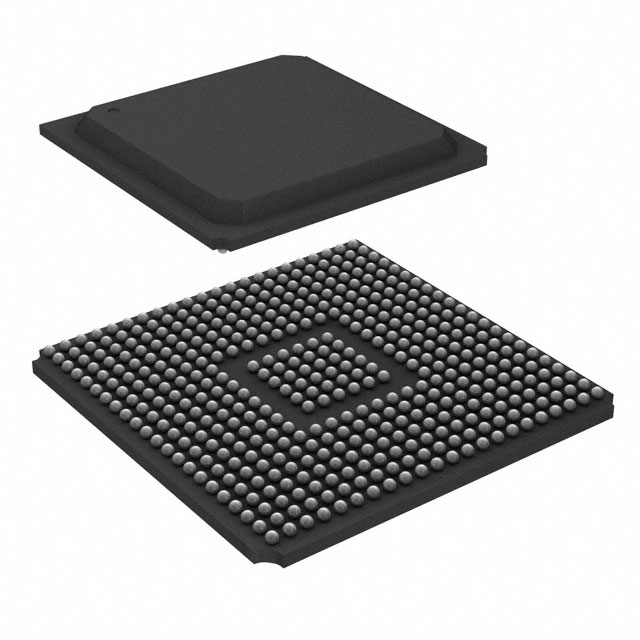
The XC2V250-4FGG456I comes in a compact package suitable for surface-mount technology (SMT) assembly. It is available in a 456-ball Fine-Pitch Ball Grid Array (FBGA) package.
Essence
The essence of the XC2V250-4FGG456I lies in its ability to provide a highly flexible and customizable solution for implementing complex digital logic functions.
Packaging/Quantity
The XC2V250-4FGG456I is typically sold individually or in small quantities, depending on the supplier's packaging options.
Specifications
- FPGA Family: Virtex-II
- Logic Cells: 250,000
- Number of I/Os: 456
- Operating Voltage: 3.3V
- Maximum Frequency: 200 MHz
- Embedded Memory: Up to 1,152 Kbits
- Configuration Memory: 4 Mbits
- Package Type: FBGA
- Package Pins: 456
Detailed Pin Configuration
The XC2V250-4FGG456I has a total of 456 pins, each serving a specific purpose in the FPGA's operation. A detailed pin configuration diagram can be found in the product datasheet provided by the manufacturer.
Functional Features
High-Speed Processing
The XC2V250-4FGG456I offers high-speed processing capabilities, making it suitable for applications that require real-time data processing and complex algorithm execution.
Flexible I/O Options
With 456 I/O pins, the XC2V250-4FGG456I provides ample flexibility for interfacing with external devices and peripherals. This allows for seamless integration into various system architectures.
Embedded Memory
The FPGA includes embedded memory blocks, providing additional storage capacity for data buffering, lookup tables, or other application-specific purposes.
Advantages and Disadvantages
Advantages
- Flexibility: The programmable nature of FPGAs allows for customization and adaptation to changing requirements.
- High performance: FPGAs offer fast processing speeds and efficient execution of complex algorithms.
- Scalability: FPGAs can be easily scaled up or down depending on the complexity of the design.
Disadvantages
- Complexity: Designing and programming FPGAs can be challenging, requiring specialized knowledge and expertise.
- Power consumption: FPGAs tend to consume more power compared to other integrated circuits, especially when operating at high frequencies.
Working Principles
FPGAs consist of an array of configurable logic blocks (CLBs) interconnected through programmable routing resources. These CLBs contain look-up tables (LUTs), flip-flops, and other components that can be configured to implement desired logic functions. The XC2V250-4FGG456I utilizes this architecture to provide flexible and customizable digital logic processing.
Detailed Application Field Plans
The XC2V250-4FGG456I finds applications in various fields, including:
- Telecommunications: Used for signal processing, protocol conversion, and network optimization.
- Aerospace and Defense: Employed in radar systems, avionics, and secure communications.
- Industrial Automation: Utilized for control systems, robotics, and machine vision.
- Medical Devices: Integrated into imaging systems, patient monitoring, and diagnostic equipment.
- Automotive: Applied in advanced driver-assistance systems (ADAS), infotainment, and engine control.
Detailed and Complete Alternative Models
- XC2V1000-4FGG456I: Similar to the XC2V250-4FGG456I but with a higher logic cell count of 1,000,000.
- XC2V500-4FGG456I: A lower-cost alternative with 500,000 logic cells, suitable for less complex applications.
- XC2V4000-4FGG456I: A high-end model with 4,000,000 logic cells, offering enhanced performance for demanding applications.
10個與XC2V250-4FGG456I在技術方案中應用相關的常見問題與解答
Sure! Here are 10 common questions and answers related to the application of XC2V250-4FGG456I in technical solutions:
Q: What is XC2V250-4FGG456I? A: XC2V250-4FGG456I is a specific model of Field Programmable Gate Array (FPGA) manufactured by Xilinx.
Q: What are the key features of XC2V250-4FGG456I? A: Some key features of XC2V250-4FGG456I include 250,000 system gates, 456-pin Fine-Pitch Ball Grid Array (FBGA) package, and support for various I/O standards.
Q: In what technical solutions can XC2V250-4FGG456I be used? A: XC2V250-4FGG456I can be used in a wide range of technical solutions, including digital signal processing, embedded systems, telecommunications, aerospace, and industrial automation.
Q: How does XC2V250-4FGG456I contribute to digital signal processing applications? A: XC2V250-4FGG456I provides high-speed processing capabilities, parallel computing, and flexibility to implement complex algorithms efficiently, making it suitable for digital signal processing applications.
Q: Can XC2V250-4FGG456I be used in safety-critical applications like aerospace or automotive systems? A: Yes, XC2V250-4FGG456I can be used in safety-critical applications. However, additional measures such as redundancy and fault-tolerant design may be required to meet the stringent reliability requirements.
Q: What development tools are available for programming XC2V250-4FGG456I? A: Xilinx provides various development tools like Vivado Design Suite and ISE Design Suite, which offer comprehensive features for designing, simulating, and programming XC2V250-4FGG456I.
Q: Can XC2V250-4FGG456I be reprogrammed after deployment? A: Yes, XC2V250-4FGG456I is a Field Programmable device, meaning it can be reprogrammed even after deployment, allowing for flexibility and adaptability in the field.
Q: What are some advantages of using XC2V250-4FGG456I in embedded systems? A: XC2V250-4FGG456I offers low power consumption, small form factor, high performance, and the ability to integrate multiple functions into a single chip, making it suitable for embedded system applications.
Q: Are there any limitations or considerations when using XC2V250-4FGG456I in technical solutions? A: Some considerations include power consumption, thermal management, I/O compatibility, and the need for expertise in FPGA design and programming.
Q: Where can I find additional resources and support for working with XC2V250-4FGG456I? A: Xilinx's official website provides documentation, application notes, forums, and technical support to assist users in working with XC2V250-4FGG456I.