

XC2C384-7PQG208C
Product Overview
Category:
The XC2C384-7PQG208C belongs to the category of complex programmable logic devices (CPLDs).
Use:
It is used for implementing digital systems in various applications such as telecommunications, automotive, industrial control, and consumer electronics.
Characteristics:
- The XC2C384-7PQG208C offers high logic density and low power consumption, making it suitable for battery-powered and portable applications.
- It features reprogrammable logic, allowing for flexibility in design iterations and updates.
- The device supports a wide range of I/O standards, enabling interfacing with different types of external components.
Package:
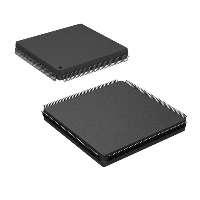
The XC2C384-7PQG208C is available in a 208-pin quad flat package (QFP), providing ease of integration into circuit boards.
Essence:
The essence of XC2C384-7PQG208C lies in its ability to efficiently implement complex digital logic functions while consuming minimal power.
Packaging/Quantity:
The XC2C384-7PQG208C is typically supplied in reels or trays, with quantities varying based on the manufacturer's packaging specifications.
Specifications
- Logic Elements: 384 macrocells
- I/O Pins: 108
- Operating Voltage: 1.8V to 3.3V
- Speed Grade: -7
- Maximum Frequency: Up to 300 MHz
Detailed Pin Configuration
The detailed pin configuration of XC2C384-7PQG208C can be found in the manufacturer's datasheet, which provides comprehensive information about the pinout and functionality of each pin.
Functional Features
- In-system programmability for on-the-fly configuration updates
- Flexible clocking resources for accommodating diverse timing requirements
- On-chip analog-to-digital converters for mixed-signal applications
- Built-in security features for protecting intellectual property
Advantages and Disadvantages
Advantages
- High logic density for implementing complex designs
- Low power consumption for energy-efficient operation
- Reprogrammable nature allows for design flexibility
- Wide range of I/O standards support diverse interfacing needs
Disadvantages
- Limited capacity compared to larger FPGA devices
- Relatively lower performance compared to high-end FPGAs
- Limited support for advanced DSP and high-speed serial interfaces
Working Principles
The XC2C384-7PQG208C operates based on the principles of configurable logic, where the internal logic elements and interconnections can be programmed to realize specific digital functions. This programming is typically done using hardware description languages (HDL) and synthesis tools, resulting in a customized configuration that defines the device's behavior.
Detailed Application Field Plans
The XC2C384-7PQG208C finds application in various fields, including: - Telecommunications: Implementing protocol processing and interface control - Automotive: Control and monitoring systems for vehicle subsystems - Industrial Control: Programmable logic controllers (PLCs) and automation equipment - Consumer Electronics: Display drivers, audio processing, and user interface control
Detailed and Complete Alternative Models
- XC2C256-7PQG208C: A lower-density CPLD with similar features
- XC2C512-7PQG208C: A higher-density CPLD offering increased logic resources
- XC2C768-7PQG208C: A CPLD with expanded capacity for more complex designs
Note: The alternative models listed above are indicative and may vary based on specific design requirements and availability.
This comprehensive entry provides an in-depth understanding of the XC2C384-7PQG208C, covering its specifications, features, applications, and alternatives within the context of complex programmable logic devices.
10個與XC2C384-7PQG208C在技術方案中應用相關的常見問題與解答
What is the XC2C384-7PQG208C?
- The XC2C384-7PQG208C is a CoolRunner-II CPLD (Complex Programmable Logic Device) from Xilinx, designed for low-power applications and high-performance logic integration.
What are the key features of XC2C384-7PQG208C?
- The key features include 384 macrocells, 288 user I/Os, 32 dedicated inputs, 8 global clock resources, and 16 x 36 dual-port RAM blocks.
What are the typical applications of XC2C384-7PQG208C?
- Typical applications include portable instrumentation, consumer electronics, power management, and general-purpose logic replacement.
What are the voltage requirements for XC2C384-7PQG208C?
- The device operates at a core voltage of 1.8V and I/O voltage of 1.5V to 3.3V.
What tools are available for programming XC2C384-7PQG208C?
- Xilinx's iMPACT programming tool and third-party programming solutions can be used to program the XC2C384-7PQG208C.
Can XC2C384-7PQG208C be used in battery-powered devices?
- Yes, the low-power characteristics of XC2C384-7PQG208C make it suitable for battery-powered devices.
What are the temperature specifications for XC2C384-7PQG208C?
- The device is specified to operate over a commercial temperature range of 0°C to 70°C and an industrial temperature range of -40°C to 85°C.
Is XC2C384-7PQG208C compatible with other Xilinx devices?
- Yes, XC2C384-7PQG208C is compatible with other Xilinx devices and can be integrated into larger FPGA-based systems.
What are the design considerations for using XC2C384-7PQG208C in high-speed applications?
- Proper signal integrity, board layout, and timing constraints should be carefully considered for high-speed applications.
Where can I find detailed technical documentation for XC2C384-7PQG208C?
- Detailed technical documentation, including datasheets and application notes, can be found on the Xilinx website or through authorized distributors.