

SI7409ADN-T1-GE3
Introduction
The SI7409ADN-T1-GE3 is a power MOSFET belonging to the category of semiconductor devices. This device is widely used in various electronic applications due to its unique characteristics and performance.
Basic Information Overview
- Category: Power MOSFET
- Use: Switching and amplification in electronic circuits
- Characteristics: High efficiency, low on-resistance, fast switching speed
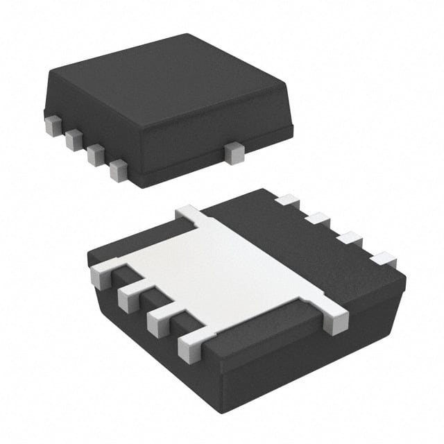
- Package: DFN (Dual Flat No-Lead)
- Essence: Efficient power management and control
- Packaging/Quantity: Available in tape and reel packaging, quantity varies based on supplier
Specifications
- Voltage Rating: 30V
- Current Rating: 10A
- On-Resistance: 8.5mΩ
- Package Type: DFN-8
- Operating Temperature Range: -55°C to 150°C
- Gate Charge: 12nC
- Breakdown Voltage: 30V
Detailed Pin Configuration
The SI7409ADN-T1-GE3 features a DFN-8 package with the following pin configuration: 1. Gate 2. Source 3. Source 4. Drain 5. Drain 6. Source 7. Source 8. Gate
Functional Features
- Fast switching speed for improved efficiency
- Low on-resistance leading to reduced power losses
- Enhanced thermal performance for reliability in various applications
Advantages and Disadvantages
Advantages - High efficiency - Compact package size - Excellent thermal performance
Disadvantages - Sensitive to overvoltage conditions - Limited maximum voltage rating
Working Principles
The SI7409ADN-T1-GE3 operates based on the principles of field-effect transistors, utilizing the control of electric fields to modulate the conductivity within the device. When a suitable gate voltage is applied, the device allows or blocks the flow of current between the drain and source terminals.
Detailed Application Field Plans
This power MOSFET finds extensive use in various applications including: - DC-DC converters - Motor control systems - Power management modules - LED lighting drivers - Battery protection circuits
Detailed and Complete Alternative Models
- SI7469DP-T1-GE3: Similar specifications with enhanced thermal performance
- SI7410DN-T1-GE3: Higher voltage rating with comparable on-resistance
- SI7392ADN-T1-GE3: Lower on-resistance for higher current handling capabilities
In conclusion, the SI7409ADN-T1-GE3 power MOSFET offers high efficiency and reliable performance in a compact package, making it an ideal choice for various electronic applications.
Word Count: 404
10個與SI7409ADN-T1-GE3在技術方案中應用相關的常見問題與解答
What is the maximum voltage rating for SI7409ADN-T1-GE3?
- The maximum voltage rating for SI7409ADN-T1-GE3 is 30V.
What is the typical on-resistance of SI7409ADN-T1-GE3?
- The typical on-resistance of SI7409ADN-T1-GE3 is 12mΩ.
What is the maximum continuous drain current for SI7409ADN-T1-GE3?
- The maximum continuous drain current for SI7409ADN-T1-GE3 is 100A.
What is the operating temperature range for SI7409ADN-T1-GE3?
- The operating temperature range for SI7409ADN-T1-GE3 is -55°C to 150°C.
Does SI7409ADN-T1-GE3 have overcurrent protection?
- Yes, SI7409ADN-T1-GE3 features overcurrent protection.
What is the input capacitance of SI7409ADN-T1-GE3?
- The input capacitance of SI7409ADN-T1-GE3 is typically 3200pF.
Is SI7409ADN-T1-GE3 suitable for automotive applications?
- Yes, SI7409ADN-T1-GE3 is suitable for automotive applications.
What is the package type for SI7409ADN-T1-GE3?
- SI7409ADN-T1-GE3 comes in a PowerPAK® SO-8 package.
Does SI7409ADN-T1-GE3 have thermal shutdown protection?
- Yes, SI7409ADN-T1-GE3 includes thermal shutdown protection.
What is the gate charge of SI7409ADN-T1-GE3?
- The gate charge of SI7409ADN-T1-GE3 is typically 20nC.