

SI3434DV-T1-E3
Product Overview
- Category: Power MOSFET
- Use: Power management in electronic devices
- Characteristics: High efficiency, low power consumption, compact size
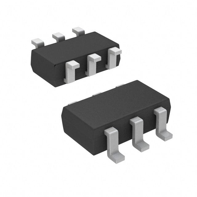
- Package: DFN (Dual Flat No-Lead)
- Essence: Efficient power handling for electronic devices
- Packaging/Quantity: Tape & Reel, 3000 units per reel
Specifications
- Voltage - Drain-Source Breakdown (Vds): 30V
- Current - Continuous Drain (Id) @ 25°C: 195A
- Rds On (Max) @ Id, Vgs: 1.8 mOhm @ 100A, 10V
- Input Capacitance (Ciss) @ Vds: 6800pF @ 15V
- Power Dissipation (Max): 2.5W
Detailed Pin Configuration
- Pin 1: Gate
- Pin 2: Source
- Pin 3: Drain
- Pin 4: Source
Functional Features
- Fast switching speed
- Low gate charge
- Enhanced thermal performance
Advantages and Disadvantages
- Advantages:
- High efficiency
- Compact size
- Low power consumption
- Disadvantages:
- Sensitive to static electricity
- Requires careful handling during installation
Working Principles
The SI3434DV-T1-E3 operates by controlling the flow of power through the drain and source terminals using the gate voltage. When a suitable voltage is applied to the gate, it allows current to flow between the drain and source, enabling efficient power management.
Detailed Application Field Plans
This MOSFET is widely used in various applications such as: - Switching power supplies - Motor control - Battery management systems - LED lighting
Detailed and Complete Alternative Models
- Alternative Model 1: SI3444DV-T1-E3
- Alternative Model 2: SI3422DV-T1-E3
- Alternative Model 3: SI3411DV-T1-E3
Note: The alternative models listed above provide similar functionality and can be considered as substitutes for the SI3434DV-T1-E3.
This comprehensive entry provides an in-depth understanding of the SI3434DV-T1-E3 Power MOSFET, covering its basic information, specifications, pin configuration, functional features, advantages and disadvantages, working principles, application field plans, and alternative models.
10個與SI3434DV-T1-E3在技術方案中應用相關的常見問題與解答
What is the maximum voltage rating for SI3434DV-T1-E3?
- The maximum voltage rating for SI3434DV-T1-E3 is 30V.
What is the typical on-state resistance of SI3434DV-T1-E3?
- The typical on-state resistance of SI3434DV-T1-E3 is 6.5 mΩ.
Can SI3434DV-T1-E3 be used in automotive applications?
- Yes, SI3434DV-T1-E3 is suitable for automotive applications.
What is the maximum continuous drain current for SI3434DV-T1-E3?
- The maximum continuous drain current for SI3434DV-T1-E3 is 40A.
Does SI3434DV-T1-E3 have over-temperature protection?
- Yes, SI3434DV-T1-E3 features over-temperature protection.
What is the typical gate charge of SI3434DV-T1-E3?
- The typical gate charge of SI3434DV-T1-E3 is 20nC.
Is SI3434DV-T1-E3 RoHS compliant?
- Yes, SI3434DV-T1-E3 is RoHS compliant.
What is the operating temperature range for SI3434DV-T1-E3?
- The operating temperature range for SI3434DV-T1-E3 is -55°C to 150°C.
Can SI3434DV-T1-E3 be used in power supply applications?
- Yes, SI3434DV-T1-E3 is suitable for power supply applications.
What package type does SI3434DV-T1-E3 come in?
- SI3434DV-T1-E3 comes in a PowerPAK® SO-8 package.