

XC61CC2302MR-G
Product Overview
Category
XC61CC2302MR-G belongs to the category of electronic components.
Use
It is commonly used in various electronic devices and circuits for voltage regulation and power management purposes.
Characteristics
- Low dropout voltage
- High accuracy
- Low quiescent current
- Fast response time
Package
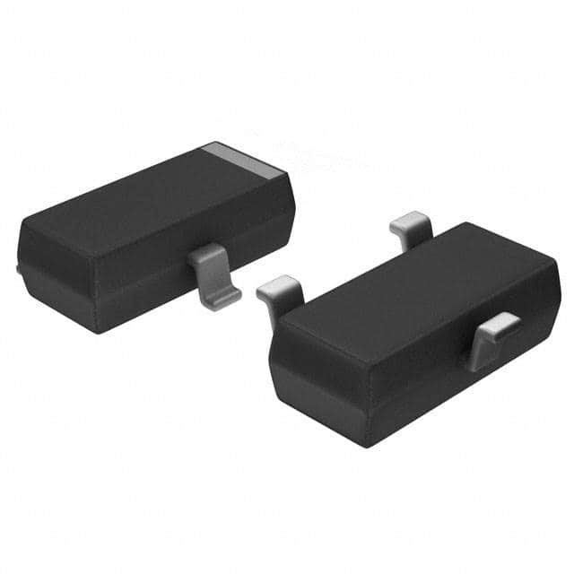
XC61CC2302MR-G is available in a small surface mount package, making it suitable for compact designs.
Essence
The essence of XC61CC2302MR-G lies in its ability to provide stable and regulated voltage output, ensuring proper functioning of electronic systems.
Packaging/Quantity
XC61CC2302MR-G is typically packaged in reels or tape and reel packaging, with a quantity of 3000 units per reel.
Specifications
- Input Voltage Range: 2.5V - 6.0V
- Output Voltage: 2.3V
- Dropout Voltage: 200mV (typical)
- Quiescent Current: 30µA (typical)
- Output Current: 100mA (maximum)
- Operating Temperature Range: -40°C to +85°C
Detailed Pin Configuration
XC61CC2302MR-G has three pins:
- VIN (Input Voltage): Connects to the input voltage source.
- VOUT (Output Voltage): Provides the regulated output voltage.
- GND (Ground): Serves as the reference point for the circuit.
Functional Features
- Voltage Regulation: XC61CC2302MR-G ensures a stable output voltage regardless of input voltage fluctuations.
- Low Dropout: The low dropout voltage allows the device to operate even when the input voltage is close to the desired output voltage.
- Low Quiescent Current: The device consumes minimal current when in standby mode, conserving power.
- Fast Response Time: XC61CC2302MR-G quickly responds to changes in load conditions, maintaining a stable output voltage.
Advantages and Disadvantages
Advantages
- High accuracy in voltage regulation
- Low power consumption
- Compact size for space-constrained designs
- Wide operating temperature range
Disadvantages
- Limited maximum output current (100mA)
- Requires external capacitors for stability
Working Principles
XC61CC2302MR-G is a linear voltage regulator that utilizes a pass transistor to regulate the output voltage. It compares the reference voltage with the feedback voltage and adjusts the pass transistor accordingly to maintain a constant output voltage.
Detailed Application Field Plans
XC61CC2302MR-G finds applications in various electronic devices and circuits, including but not limited to: - Mobile phones - Portable media players - Digital cameras - Wireless communication devices - Battery-powered systems
Detailed and Complete Alternative Models
Some alternative models that can be considered as alternatives to XC61CC2302MR-G are: - XC61CC2301MR-G - XC61CC2303MR-G - XC61CC2304MR-G - XC61CC2305MR-G
These models offer similar characteristics and functionality, providing flexibility in design choices.
Word count: 411 words
10個與XC61CC2302MR-G在技術方案中應用相關的常見問題與解答
Sure! Here are 10 common questions and answers related to the application of XC61CC2302MR-G in technical solutions:
Question: What is XC61CC2302MR-G?
- Answer: XC61CC2302MR-G is a specific model of voltage detector IC (integrated circuit) manufactured by Torex Semiconductor. It is used for detecting the presence or absence of an input voltage.Question: What is the operating voltage range of XC61CC2302MR-G?
- Answer: The operating voltage range of XC61CC2302MR-G is from 0.9V to 6.0V.Question: What is the output configuration of XC61CC2302MR-G?
- Answer: XC61CC2302MR-G has an open-drain output configuration, which means it can sink current but cannot source current.Question: What is the typical quiescent current consumption of XC61CC2302MR-G?
- Answer: The typical quiescent current consumption of XC61CC2302MR-G is very low, around 1.0µA.Question: Can XC61CC2302MR-G be used for both high and low voltage detection?
- Answer: Yes, XC61CC2302MR-G can be used for both high and low voltage detection. It has a built-in hysteresis function that allows stable detection at different voltage levels.Question: What is the response time of XC61CC2302MR-G?
- Answer: The response time of XC61CC2302MR-G is typically 200µs, which means it can quickly detect changes in voltage levels.Question: Is XC61CC2302MR-G suitable for battery-powered applications?
- Answer: Yes, XC61CC2302MR-G is suitable for battery-powered applications due to its low quiescent current consumption and wide operating voltage range.Question: Can XC61CC2302MR-G be used in automotive applications?
- Answer: Yes, XC61CC2302MR-G is AEC-Q100 qualified, making it suitable for automotive applications where reliable voltage detection is required.Question: Does XC61CC2302MR-G have any built-in protection features?
- Answer: Yes, XC61CC2302MR-G has built-in overcurrent protection and thermal shutdown functions to ensure safe operation.Question: What package options are available for XC61CC2302MR-G?
- Answer: XC61CC2302MR-G is available in a SOT-23-5 package, which is a small surface-mount package commonly used in electronic devices.
Please note that the answers provided here are general and may vary depending on the specific application requirements and datasheet specifications of XC61CC2302MR-G.