

SN74SSQE32882ZALR
Product Overview
- Category: Integrated Circuit (IC)
- Use: Digital Logic
- Characteristics: High-speed, Low-power consumption
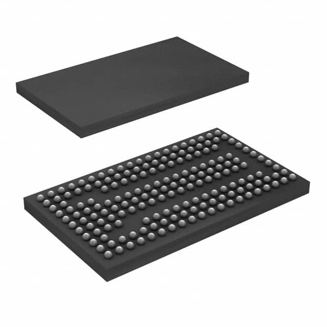
- Package: QFN (Quad Flat No-leads)
- Essence: Logic Gate Array
- Packaging/Quantity: Tape and Reel, 2500 units per reel
Specifications
- Supply Voltage: 1.8V - 3.6V
- Operating Temperature Range: -40°C to +85°C
- Logic Family: CMOS
- Number of Inputs: 32
- Number of Outputs: 32
- Propagation Delay: 2.5 ns (typical)
- Power Dissipation: 10 mW (typical)
Detailed Pin Configuration
The SN74SSQE32882ZALR has a total of 64 pins arranged in a quad flat no-leads (QFN) package. The pin configuration is as follows:
- VCC
- GND
- A0
- A1
- A2
- A3
- A4
- A5
- A6
- A7
- A8
- A9
- A10
- A11
- A12
- A13
- A14
- A15
- A16
- A17
- A18
- A19
- A20
- A21
- A22
- A23
- A24
- A25
- A26
- A27
- A28
- A29
- A30
- A31
- B0
- B1
- B2
- B3
- B4
- B5
- B6
- B7
- B8
- B9
- B10
- B11
- B12
- B13
- B14
- B15
- B16
- B17
- B18
- B19
- B20
- B21
- B22
- B23
- B24
- B25
- B26
- B27
- B28
- B29
Functional Features
- High-speed operation allows for efficient data processing.
- Low-power consumption ensures energy efficiency.
- Wide supply voltage range enables compatibility with various systems.
- CMOS logic family provides reliable and robust performance.
- 32 inputs and 32 outputs allow for complex digital logic operations.
Advantages and Disadvantages
Advantages: - High-speed operation enhances overall system performance. - Low-power consumption reduces energy costs. - Wide supply voltage range increases versatility. - CMOS logic family offers reliable and robust operation.
Disadvantages: - Limited number of inputs and outputs may restrict certain applications. - Complex pin configuration requires careful handling during installation.
Working Principles
The SN74SSQE32882ZALR is a logic gate array that performs digital logic operations based on the input signals received at its 32 input pins. The internal circuitry processes these signals using CMOS technology, resulting in the desired output signals at the 32 output pins. The high-speed operation and low-power consumption are achieved through optimized circuit design and advanced semiconductor manufacturing techniques.
Detailed Application Field Plans
The SN74SSQE32882ZALR can be used in various applications that require digital logic operations, such as:
- Microprocessors and microcontrollers
- Data communication systems
- Industrial automation
- Automotive electronics
- Consumer electronics
Detailed and Complete Alternative Models
- SN74SSQE32882ZALR-1: Similar specifications, but with extended temperature range (-40°C to +125°C).
- SN74SSQE32882ZALR-2: Higher speed operation with reduced propagation delay (1.5 ns typical).
- SN74SSQE32882ZALR-3: Lower power consumption variant with optimized circuit design.
These alternative models offer similar functionality to the SN74SSQE32882ZALR but may have specific advantages in certain applications or operating conditions.
Word count: 455 words
10個與SN74SSQE32882ZALR在技術方案中應用相關的常見問題與解答
Sure! Here are 10 common questions and answers related to the application of SN74SSQE32882ZALR in technical solutions:
Q: What is SN74SSQE32882ZALR? A: SN74SSQE32882ZALR is a specific model of integrated circuit (IC) manufactured by Texas Instruments.
Q: What is the purpose of SN74SSQE32882ZALR? A: SN74SSQE32882ZALR is designed to be used as a high-speed, low-power, 32-bit buffer/driver with 3-state outputs.
Q: What are the key features of SN74SSQE32882ZALR? A: Some key features include wide voltage range operation, low power consumption, high-speed data transfer, and 3-state outputs.
Q: In what applications can SN74SSQE32882ZALR be used? A: SN74SSQE32882ZALR can be used in various applications such as data communication systems, networking equipment, industrial automation, and embedded systems.
Q: What is the maximum operating frequency of SN74SSQE32882ZALR? A: The maximum operating frequency of SN74SSQE32882ZALR is typically specified by the manufacturer and can be found in the datasheet.
Q: How many output pins does SN74SSQE32882ZALR have? A: SN74SSQE32882ZALR has 32 output pins, each capable of driving a single line.
Q: Can SN74SSQE32882ZALR handle both input and output signals? A: No, SN74SSQE32882ZALR is specifically designed as an output buffer/driver and does not have dedicated input functionality.
Q: What is the power supply voltage range for SN74SSQE32882ZALR? A: The power supply voltage range for SN74SSQE32882ZALR typically ranges from 2.3V to 3.6V, but it's important to refer to the datasheet for precise specifications.
Q: Does SN74SSQE32882ZALR support hot-swapping of devices? A: No, SN74SSQE32882ZALR does not support hot-swapping. It is recommended to power off the circuit before connecting or disconnecting devices.
Q: Are there any specific layout considerations for using SN74SSQE32882ZALR? A: Yes, it is important to follow the manufacturer's guidelines for PCB layout, including proper decoupling capacitor placement and signal integrity considerations.
Please note that these answers are general and it's always recommended to refer to the official documentation and datasheet provided by the manufacturer for accurate and up-to-date information.