

SN74LVC245ADGVR
Overview
- Category: Integrated Circuit
- Use: Level Shifter/Transceiver
- Characteristics: Bi-directional, 8-bit, voltage level translation
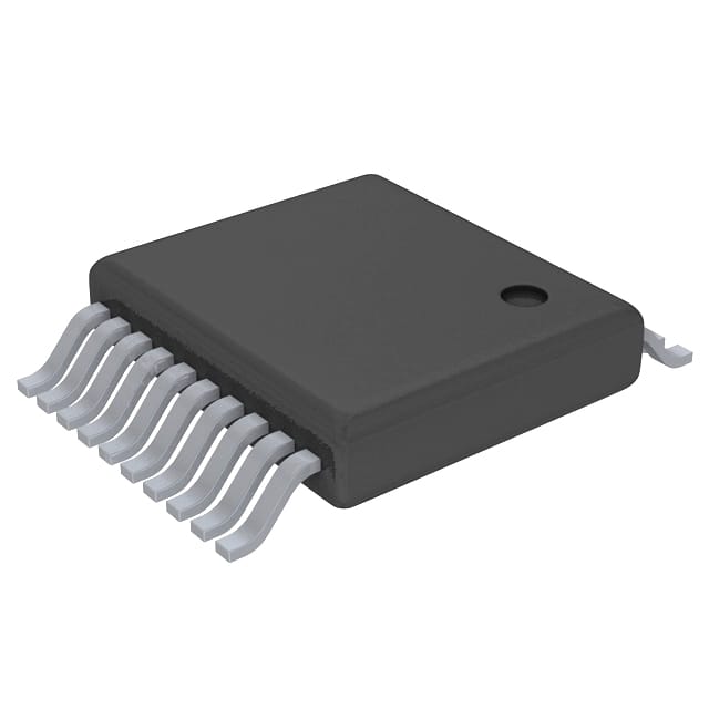
- Package: TSSOP-20
- Essence: Transfers data between different voltage domains
- Packaging/Quantity: Tape and Reel, 2500 pieces per reel
Specifications
- Supply Voltage Range: 1.65V to 5.5V
- High-Level Input Voltage: 2V to VCC + 0.5V
- Low-Level Input Voltage: -0.5V to 0.8V
- High-Level Output Voltage: VCC - 0.4V
- Low-Level Output Voltage: 0.4V
- Maximum Operating Frequency: 80MHz
- Propagation Delay: 3.6ns (Max)
- Operating Temperature Range: -40°C to 85°C
Pin Configuration
The SN74LVC245ADGVR has a total of 20 pins. The pin configuration is as follows:
- OE (Output Enable) 1
- A1 (Data Input/Output) 1
- B1 (Data Input/Output) 1
- A2 (Data Input/Output) 2
- B2 (Data Input/Output) 2
- A3 (Data Input/Output) 3
- B3 (Data Input/Output) 3
- A4 (Data Input/Output) 4
- B4 (Data Input/Output) 4
- GND (Ground)
- B5 (Data Input/Output) 5
- A5 (Data Input/Output) 5
- B6 (Data Input/Output) 6
- A6 (Data Input/Output) 6
- B7 (Data Input/Output) 7
- A7 (Data Input/Output) 7
- B8 (Data Input/Output) 8
- A8 (Data Input/Output) 8
- VCC (Supply Voltage)
- OE (Output Enable) 2
Functional Features
The SN74LVC245ADGVR is a bi-directional level shifter/transceiver integrated circuit. It allows for the bidirectional transfer of data between two voltage domains. The device can operate with a supply voltage ranging from 1.65V to 5.5V, making it compatible with a wide range of systems.
The output enable (OE) pins control the direction of data flow. When OE is low, the device is in the active state, and data can be transferred bidirectionally. When OE is high, the device is in the high-impedance state, and data transfer is disabled.
The SN74LVC245ADGVR features 8-bit data input/output ports (A1-A8 and B1-B8), allowing for the simultaneous transfer of 8 bits of data. The device also has built-in protection against bus contention, ensuring that no damage occurs when multiple drivers attempt to drive the bus simultaneously.
Advantages and Disadvantages
Advantages: - Bi-directional data transfer between different voltage domains - Wide supply voltage range allows for compatibility with various systems - Built-in protection against bus contention
Disadvantages: - Propagation delay of 3.6ns may limit its use in high-speed applications - Limited number of data input/output ports (8 bits)
Working Principles
The SN74LVC245ADGVR operates by using a combination of MOSFETs and CMOS logic to perform voltage level translation. When the OE pin is low, the device acts as a bidirectional buffer, allowing data to flow between the A and B ports. The MOSFETs ensure that the voltage levels of the input and output signals are properly translated.
The device also incorporates protection circuitry to prevent damage in case of bus contention. This ensures that only one driver is actively driving the bus at any given time, preventing conflicts and potential damage to the integrated circuit or the connected systems.
Detailed Application Field Plans
The SN74LVC245ADGVR can be used in various applications where voltage level translation is required. Some potential application fields include:
- Microcontroller Interfacing: The device can be used to interface microcontrollers operating at different voltage levels, allowing them to communicate with each other.
- Communication Systems: It can be used in communication systems to enable data transfer between devices operating at different voltage domains, such as UART, SPI, or I2C interfaces.
- Battery-Powered Devices: The wide supply voltage range makes it suitable for use in battery-powered devices, where different voltage levels may be
10個與SN74LVC245ADGVR在技術方案中應用相關的常見問題與解答
Sure! Here are 10 common questions and answers related to the application of SN74LVC245ADGVR:
Q: What is SN74LVC245ADGVR? A: SN74LVC245ADGVR is a bidirectional octal bus transceiver with 3-state outputs, commonly used for level shifting and voltage translation in digital systems.
Q: What is the operating voltage range of SN74LVC245ADGVR? A: The operating voltage range is from 1.65V to 5.5V, making it compatible with a wide range of digital logic levels.
Q: How many channels does SN74LVC245ADGVR have? A: SN74LVC245ADGVR has 8 bidirectional channels, allowing for parallel data transfer between two buses.
Q: Can SN74LVC245ADGVR handle high-speed data transmission? A: Yes, SN74LVC245ADGVR is designed to support high-speed data transmission up to 100 MHz.
Q: What is the maximum output current of SN74LVC245ADGVR? A: The maximum output current per channel is 32 mA, which allows for driving standard CMOS or TTL loads.
Q: Does SN74LVC245ADGVR have built-in ESD protection? A: Yes, SN74LVC245ADGVR has built-in ESD protection, ensuring robustness against electrostatic discharge events.
Q: Can SN74LVC245ADGVR be used for level shifting between different voltage domains? A: Yes, SN74LVC245ADGVR can be used for level shifting between voltage domains, as long as the voltage levels are within its operating range.
Q: Does SN74LVC245ADGVR support 3-state outputs? A: Yes, SN74LVC245ADGVR supports 3-state outputs, allowing for bus sharing and multi-master systems.
Q: What is the typical propagation delay of SN74LVC245ADGVR? A: The typical propagation delay is around 4.1 ns, making it suitable for high-speed applications.
Q: Can SN74LVC245ADGVR be used in both commercial and industrial temperature ranges? A: Yes, SN74LVC245ADGVR is available in both commercial (0°C to 70°C) and industrial (-40°C to 85°C) temperature ranges, providing flexibility for various applications.
Please note that these answers are general and may vary depending on the specific requirements and datasheet of SN74LVC245ADGVR.