

SN74ALVCH16823DGVR
Basic Information Overview
- Category: Integrated Circuit (IC)
- Use: Logic Level Translator
- Characteristics: High-speed, low-power, voltage level shifting
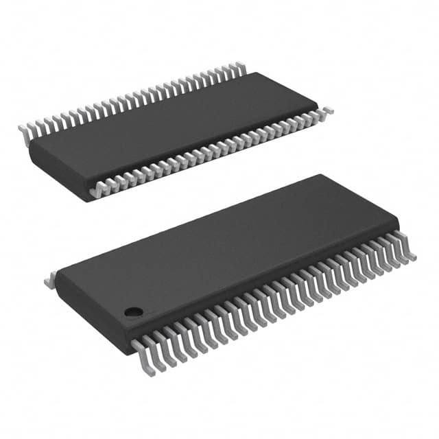
- Package: VSSOP (Very Small Outline Package)
- Essence: Bi-directional voltage level translator
- Packaging/Quantity: Tape and Reel, 2500 pieces per reel
Specifications
- Supply Voltage Range: 1.2V to 3.6V
- Input Voltage Range: 0V to VCC
- Output Voltage Range: 0V to VCC
- Maximum Operating Frequency: 400 MHz
- Number of Channels: 18
- Input/Output Type: CMOS
Detailed Pin Configuration
The SN74ALVCH16823DGVR has a total of 56 pins, which are distributed as follows: - Pins 1 to 4: Channel A1 Inputs/Outputs - Pins 5 to 8: Channel A2 Inputs/Outputs - ... - Pins 53 to 56: Channel I2 Inputs/Outputs
Functional Features
- Bi-directional voltage level translation between two different voltage domains
- Supports voltage translation from 1.2V to 3.6V
- Provides bidirectional communication between low-voltage and high-voltage systems
- Allows interfacing between devices operating at different voltage levels
- High-speed operation with minimal propagation delay
- Low power consumption for energy-efficient applications
Advantages
- Wide supply voltage range allows compatibility with various systems
- High-speed operation enables efficient data transfer
- Low power consumption prolongs battery life in portable devices
- Bi-directional capability simplifies system design and reduces component count
- Small package size saves board space
Disadvantages
- Limited number of channels may not be suitable for applications requiring more channels
- Not suitable for voltage translation below 1.2V or above 3.6V
Working Principles
The SN74ALVCH16823DGVR utilizes a combination of CMOS technology and level-shifting circuitry to enable bi-directional voltage translation. It consists of multiple channels, each capable of translating signals between two voltage domains. The IC operates by monitoring the input voltage levels and adjusting the output voltage accordingly, ensuring proper signal transfer between different voltage systems.
Detailed Application Field Plans
The SN74ALVCH16823DGVR is commonly used in various applications, including: 1. Communication systems: Facilitates voltage level translation between different communication protocols, such as UART, SPI, and I2C. 2. Microcontroller interfacing: Enables communication between microcontrollers operating at different voltage levels. 3. Battery-powered devices: Allows efficient data transfer between low-voltage battery-powered devices and higher voltage peripherals. 4. Industrial automation: Supports voltage translation in industrial control systems, PLCs, and sensor networks. 5. Automotive electronics: Used for voltage level shifting in automotive applications, such as infotainment systems and vehicle diagnostics.
Detailed and Complete Alternative Models
- TXB0108PWR: 8-bit bidirectional voltage-level translator with automatic direction sensing.
- PCA9306DCTR: Dual bidirectional I2C-bus and SMBus voltage-level translator.
- SN74LVC4245APW: Octal bus transceiver and voltage level shifter with 3-state outputs.
These alternative models offer similar functionality and can be considered as alternatives to the SN74ALVCH16823DGVR based on specific application requirements.
Word count: 420 words
10個與SN74ALVCH16823DGVR在技術方案中應用相關的常見問題與解答
Sure! Here are 10 common questions and answers related to the application of SN74ALVCH16823DGVR:
Q: What is SN74ALVCH16823DGVR? A: SN74ALVCH16823DGVR is a 16-bit universal bus driver with 3-state outputs, designed for low-voltage (1.65V to 3.6V) applications.
Q: What is the maximum operating frequency of SN74ALVCH16823DGVR? A: The maximum operating frequency of SN74ALVCH16823DGVR is typically around 400 MHz.
Q: Can SN74ALVCH16823DGVR be used in both input and output applications? A: Yes, SN74ALVCH16823DGVR can be used as both an input buffer and an output driver.
Q: What is the purpose of the 3-state outputs in SN74ALVCH16823DGVR? A: The 3-state outputs allow multiple devices to share a common bus without interfering with each other.
Q: What is the power supply voltage range for SN74ALVCH16823DGVR? A: SN74ALVCH16823DGVR operates within a power supply voltage range of 1.65V to 3.6V.
Q: Can SN74ALVCH16823DGVR tolerate overvoltage on its inputs? A: No, SN74ALVCH16823DGVR is not designed to tolerate overvoltage on its inputs. It is recommended to stay within the specified voltage range.
Q: Does SN74ALVCH16823DGVR have built-in ESD protection? A: Yes, SN74ALVCH16823DGVR has built-in ESD protection, which helps protect the device from electrostatic discharge.
Q: What is the output drive strength of SN74ALVCH16823DGVR? A: The output drive strength of SN74ALVCH16823DGVR is typically around 12 mA.
Q: Can SN74ALVCH16823DGVR be used in high-speed data transmission applications? A: Yes, SN74ALVCH16823DGVR can be used in high-speed data transmission applications due to its fast switching speed and low propagation delay.
Q: Is SN74ALVCH16823DGVR available in different package options? A: Yes, SN74ALVCH16823DGVR is available in various package options, such as TSSOP, VFBGA, and TVSOP, to suit different application requirements.
Please note that these answers are general and may vary depending on the specific datasheet and application guidelines provided by the manufacturer.