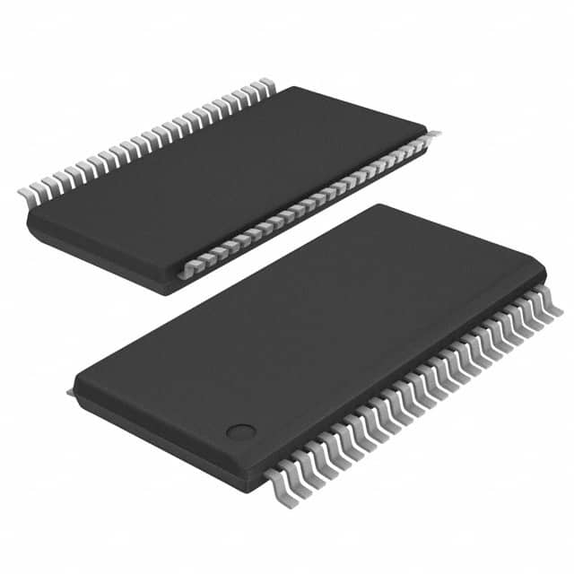
Encyclopedia Entry: 74ALB16244DGVRG4
Product Information Overview
Category: Integrated Circuit (IC)
Use: The 74ALB16244DGVRG4 is a high-performance, low-power, 16-bit buffer/driver with 3-state outputs. It is designed to provide buffering and signal amplification for digital circuits.
Characteristics: This IC operates at a voltage range of 2.0V to 3.6V and has a maximum output current of ±24mA. It features a symmetrical output impedance with both sourcing and sinking capabilities. The 74ALB16244DGVRG4 is known for its high-speed operation, low power consumption, and compatibility with various logic families.
Package: The 74ALB16244DGVRG4 is available in a small-footprint TSSOP-48 package, which offers excellent thermal performance and ease of integration into circuit boards.
Essence: The essence of the 74ALB16244DGVRG4 lies in its ability to provide reliable signal buffering and driving capabilities for digital circuits, ensuring proper signal propagation and integrity.
Packaging/Quantity: The 74ALB16244DGVRG4 is typically sold in reels or tubes, with each reel containing 2500 units or each tube containing 90 units.
Specifications
- Supply Voltage Range: 2.0V to 3.6V
- Input Voltage Range: 0V to VCC
- Output Voltage Range: 0V to VCC
- Maximum Output Current: ±24mA
- Operating Temperature Range: -40°C to +85°C
- Logic Family Compatibility: TTL, CMOS
Detailed Pin Configuration
The 74ALB16244DGVRG4 has a total of 48 pins, arranged as follows:
+---------------------+
   OE1 | 1               48 | VCC
   A1  | 2               47 | B1
   Y1  | 3               46 | GND
   A2  | 4               45 | B2
   Y2  | 5               44 | G1
   A3  | 6               43 | B3
   Y3  | 7               42 | G2
   A4  | 8               41 | B4
   Y4  | 9               40 | G3
   A5  | 10              39 | B5
   Y5  | 11              38 | G4
   A6  | 12              37 | B6
   Y6  | 13              36 | G5
   A7  | 14              35 | B7
   Y7  | 15              34 | G6
   A8  | 16              33 | B8
   Y8  | 17              32 | G7
   A9  | 18              31 | B9
   Y9  | 19              30 | G8
   A10 | 20              29 | B10
   Y10 | 21              28 | G9
   A11 | 22              27 | B11
   Y11 | 23              26 | G10
   A12 | 24              25 | B12
       +---------------------+
Functional Features
- High-speed operation: The 74ALB16244DGVRG4 can handle high-frequency signals, making it suitable for applications requiring fast data transfer.
- Low power consumption: This IC is designed to minimize power consumption, making it ideal for battery-powered devices and energy-efficient systems.
- 3-state outputs: The 74ALB16244DGVRG4 features 3-state outputs, allowing multiple devices to share a common bus without interference.
- Symmetrical output impedance: The IC provides balanced sourcing and sinking capabilities, ensuring signal integrity in both directions.
Advantages and Disadvantages
Advantages: - High-speed operation enables efficient data transfer. - Low power consumption prolongs battery life and reduces energy costs. - 3-state outputs facilitate bus sharing and system integration. - Symmetrical output impedance ensures signal integrity.
Disadvantages: - Limited voltage range (2.0V to 3.6V) may not be suitable for all applications. - TSSOP-48 package may require careful handling during assembly.
Working Principles
The 74ALB16244DGVRG4 operates as a buffer/driver by receiving input signals and amplifying them to drive downstream components or circuits. It utilizes internal circuitry to provide high-speed signal propagation, low power consumption, and symmetrical output impedance
10個與74ALB16244DGVRG4在技術方案中應用相關的常見問題與解答
Sure! Here are 10 common questions and answers related to the application of 74ALB16244DGVRG4 in technical solutions:
Q: What is the 74ALB16244DGVRG4? A: The 74ALB16244DGVRG4 is a 16-bit buffer/driver with 3-state outputs, designed for high-performance applications.
Q: What is the maximum operating voltage for the 74ALB16244DGVRG4? A: The maximum operating voltage for the 74ALB16244DGVRG4 is typically 3.6V.
Q: What is the output current capability of the 74ALB16244DGVRG4? A: The 74ALB16244DGVRG4 has a typical output current capability of ±24mA.
Q: Can the 74ALB16244DGVRG4 be used as a level shifter? A: Yes, the 74ALB16244DGVRG4 can be used as a level shifter to convert signals between different voltage levels.
Q: What is the propagation delay of the 74ALB16244DGVRG4? A: The propagation delay of the 74ALB16244DGVRG4 is typically around 3.5ns.
Q: Is the 74ALB16244DGVRG4 compatible with other logic families? A: Yes, the 74ALB16244DGVRG4 is compatible with various logic families such as TTL, CMOS, and LVTTL.
Q: Can the 74ALB16244DGVRG4 be used in bidirectional data transfer applications? A: No, the 74ALB16244DGVRG4 is a unidirectional buffer/driver and does not support bidirectional data transfer.
Q: What is the power supply voltage range for the 74ALB16244DGVRG4? A: The power supply voltage range for the 74ALB16244DGVRG4 is typically between 2.3V and 3.6V.
Q: Does the 74ALB16244DGVRG4 have built-in ESD protection? A: Yes, the 74ALB16244DGVRG4 has built-in ESD protection to safeguard against electrostatic discharge.
Q: Can the 74ALB16244DGVRG4 drive capacitive loads? A: Yes, the 74ALB16244DGVRG4 can drive capacitive loads up to a certain limit specified in the datasheet.
Please note that the answers provided here are general and may vary depending on the specific application and conditions. It's always recommended to refer to the datasheet and consult with technical experts for accurate information.


