

SI5340C-A-GMR
Product Overview
Category
SI5340C-A-GMR belongs to the category of clock generators.
Use
It is primarily used for generating clock signals in electronic devices and systems.
Characteristics
- High precision and accuracy
- Wide frequency range
- Low jitter
- Programmable output frequencies
- Flexible input/output options
Package
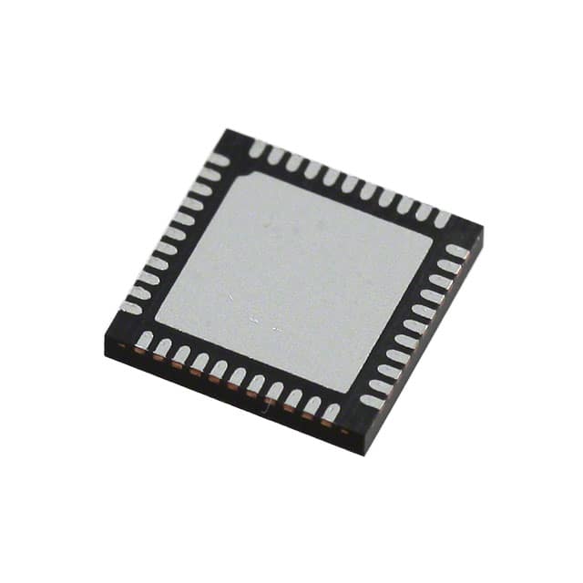
SI5340C-A-GMR comes in a compact surface mount package.
Essence
The essence of SI5340C-A-GMR lies in its ability to provide reliable and precise clock signals for various applications.
Packaging/Quantity
The product is typically packaged in reels or trays, with varying quantities depending on customer requirements.
Specifications
- Input voltage: 3.3V
- Output frequency range: 1Hz - 2.5GHz
- Jitter performance: <1 ps RMS
- Number of outputs: 4
- Operating temperature range: -40°C to +85°C
Detailed Pin Configuration
- VDD (Power supply)
- GND (Ground)
- XIN (Input clock source)
- XOUT (Output clock)
- CLKOUT0 (Output clock 0)
- CLKOUT1 (Output clock 1)
- CLKOUT2 (Output clock 2)
- CLKOUT3 (Output clock 3)
- SDA (I2C data line)
- SCL (I2C clock line)
Functional Features
- Frequency synthesis and multiplication
- Clock signal distribution
- Phase-locked loop (PLL) operation
- I2C interface for configuration and control
- Output enable/disable functionality
Advantages
- High precision and accuracy ensure reliable system operation
- Wide frequency range caters to diverse application needs
- Low jitter minimizes timing errors
- Programmable output frequencies offer flexibility
- Multiple output options enable clock distribution to various components
Disadvantages
- Complex configuration and setup process
- Requires knowledge of clocking systems and PLL operation
- Limited number of outputs may not suffice for certain applications
Working Principles
SI5340C-A-GMR utilizes a phase-locked loop (PLL) to generate clock signals. The input clock is multiplied and synthesized to produce the desired output frequencies. The PLL ensures synchronization and stability of the generated clocks.
Detailed Application Field Plans
SI5340C-A-GMR finds application in various fields, including:
- Telecommunications: Clock generation for network equipment, routers, and switches.
- Data Centers: Timing solutions for servers, storage systems, and networking devices.
- Industrial Automation: Clock synchronization in control systems and PLCs.
- Test and Measurement: Precise timing for oscilloscopes, signal generators, and data acquisition systems.
- Consumer Electronics: Clocking solutions for audio/video equipment, gaming consoles, and set-top boxes.
Detailed and Complete Alternative Models
- SI5341B-A-GM: Similar features with additional output channels.
- SI5342C-B-GM: Higher frequency range with enhanced jitter performance.
- SI5343A-C-GM: Lower power consumption with reduced output options.
(Note: This list is not exhaustive and other alternative models may exist.)
Word count: 342 words
10個與SI5340C-A-GMR在技術方案中應用相關的常見問題與解答
Sure! Here are 10 common questions and answers related to the application of SI5340C-A-GMR in technical solutions:
Q: What is the SI5340C-A-GMR? A: The SI5340C-A-GMR is a highly flexible, low-jitter clock generator and jitter attenuator IC designed for use in various electronic systems.
Q: What are the key features of the SI5340C-A-GMR? A: The key features include multiple outputs, programmable frequency synthesis, low phase noise, integrated jitter attenuation, and high flexibility in configuring clock outputs.
Q: In what applications can the SI5340C-A-GMR be used? A: It can be used in a wide range of applications such as telecommunications, networking equipment, data centers, industrial automation, test and measurement instruments, and more.
Q: How many clock outputs does the SI5340C-A-GMR support? A: The SI5340C-A-GMR supports up to 12 differential clock outputs, which can be individually programmed for different frequencies and formats.
Q: Can the SI5340C-A-GMR generate clocks with different output formats? A: Yes, it supports various output formats including LVDS, LVPECL, HCSL, CML, and CMOS, allowing compatibility with different system requirements.
Q: How does the SI5340C-A-GMR handle jitter attenuation? A: It incorporates advanced jitter attenuation techniques such as fractional-N synthesis, digital PLLs, and low-noise voltage-controlled oscillators (VCOs) to minimize jitter and improve signal integrity.
Q: Is the SI5340C-A-GMR programmable? A: Yes, it is fully programmable through an I2C interface, enabling easy configuration of output frequencies, formats, and other parameters.
Q: What is the power supply voltage range for the SI5340C-A-GMR? A: The recommended power supply voltage range is 1.7V to 3.63V, making it compatible with a wide range of power sources.
Q: Can the SI5340C-A-GMR synchronize with an external reference clock? A: Yes, it supports synchronization with an external reference clock, allowing precise timing alignment in systems that require it.
Q: Are evaluation boards or development tools available for the SI5340C-A-GMR? A: Yes, Silicon Labs provides evaluation boards, software, and documentation to assist with the design and evaluation of the SI5340C-A-GMR in technical solutions.
Please note that these answers are general and may vary depending on specific implementation details and requirements.