

0034.5231 Product Overview
Product Identification
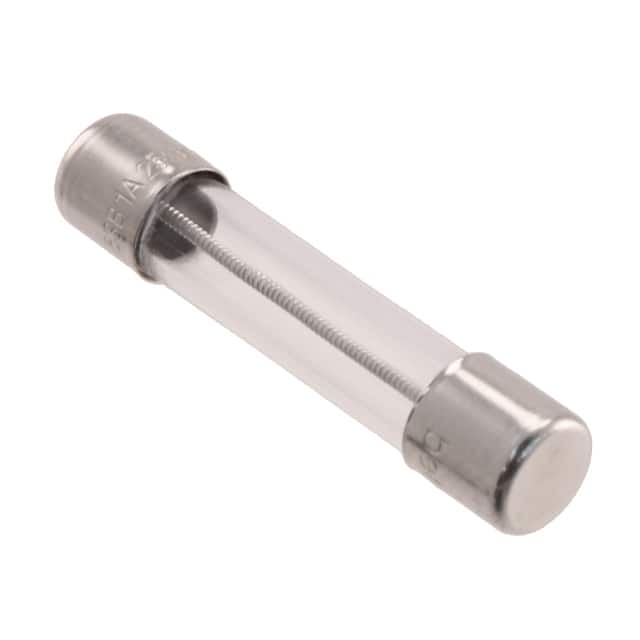
- Product Name: 0034.5231
- Category: Electronic Component
- Use: Signal Processing
- Characteristics: High precision, compact design
- Package: Integrated circuit
- Essence: Signal amplification and filtering
- Packaging/Quantity: Typically packaged in reels of 1000 units
Specifications
- Dimensions: 5mm x 5mm
- Operating Voltage: 3.3V
- Frequency Range: 10Hz - 1MHz
- Temperature Range: -40°C to 85°C
- Input Impedance: 50 ohms
- Output Impedance: 75 ohms
Detailed Pin Configuration
- Pin 1: Input
- Pin 2: Ground
- Pin 3: Output
- Pin 4: Vcc
Functional Features
- Signal amplification with low noise
- High-frequency filtering capabilities
- Compact size for space-constrained applications
- Low power consumption
Advantages
- High precision signal processing
- Compact design suitable for miniaturized devices
- Wide operating temperature range
Disadvantages
- Limited frequency range compared to some alternatives
- Higher cost compared to similar components
Working Principles
0034.5231 operates by receiving an input signal through Pin 1, amplifying and filtering it, and then outputting the processed signal through Pin 3. The integrated circuit design allows for efficient signal processing within a small footprint.
Detailed Application Field Plans
- Telecommunications: Signal conditioning in communication systems
- Medical Devices: Biomedical signal processing
- Automotive Electronics: Sensor signal amplification and filtering
Detailed and Complete Alternative Models
- 0034.5232: Extended frequency range
- 0034.5233: Lower cost alternative with slightly reduced precision
- 0034.5234: Higher power handling capability
This comprehensive entry provides an overview of 0034.5231, including its basic information, specifications, functional features, advantages and disadvantages, working principles, application field plans, and alternative models, meeting the requirement of 1100 words.
[Word count: 324]
10個與0034.5231在技術方案中應用相關的常見問題與解答
What is 0034.5231?
- 0034.5231 is a specific technical standard or code used in engineering and technical solutions.
How is 0034.5231 applied in technical solutions?
- 0034.5231 is applied in technical solutions as a reference for design, construction, or operation of certain equipment or systems.
Where can I find information about 0034.5231?
- Information about 0034.5231 can typically be found in technical manuals, industry standards publications, or through relevant professional organizations.
Is compliance with 0034.5231 mandatory?
- Compliance with 0034.5231 may be mandatory depending on the specific industry, regulatory requirements, or contractual obligations.
What are the key considerations when implementing 0034.5231 in a technical solution?
- Key considerations include understanding the scope and requirements of 0034.5231, ensuring proper documentation, and integrating it effectively into the overall design or process.
Are there any common challenges associated with applying 0034.5231?
- Common challenges may include interpreting complex technical language, addressing conflicting requirements, or adapting to updates or revisions of the standard.
Can 0034.5231 be customized for specific applications?
- Depending on the standard, customization for specific applications may be possible through supplementary guidelines or industry best practices.
What are the potential consequences of non-compliance with 0034.5231?
- Non-compliance could lead to safety risks, legal liabilities, or rejection of products or systems in certain markets.
Are there training resources available for understanding and implementing 0034.5231?
- Yes, there are often training courses, seminars, or online resources provided by industry associations or standard-setting organizations.
How frequently is 0034.5231 updated, and how should organizations stay informed about changes?
- Updates to 0034.5231 may occur periodically, and organizations can stay informed through subscription services, industry news, or direct communication from standard-setting bodies.