

NLX1G332CMX1TCG
Product Overview
Category: Integrated Circuit (IC)
Use: The NLX1G332CMX1TCG is a versatile logic gate that can be used in various digital circuit applications.
Characteristics: - Low power consumption - High-speed operation - Wide operating voltage range - Compact size
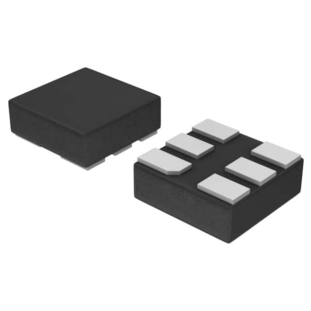
Package: The NLX1G332CMX1TCG is available in a small surface-mount package, making it suitable for space-constrained designs.
Essence: This IC serves as a fundamental building block for digital circuits, enabling logical operations such as AND, OR, and NOT.
Packaging/Quantity: The NLX1G332CMX1TCG is typically sold in reels or tubes, with each reel/tube containing a specific quantity of ICs.
Specifications
The NLX1G332CMX1TCG has the following specifications:
- Supply Voltage Range: 1.65V to 5.5V
- Input Voltage Range: 0V to VCC
- Operating Temperature Range: -40°C to +85°C
- Propagation Delay: <10ns
- Output Drive Capability: 32mA
Pin Configuration
The NLX1G332CMX1TCG features a standard pin configuration with the following pins:
- A Input
- B Input
- Y Output
- GND (Ground)
- VCC (Supply Voltage)
Functional Features
The NLX1G332CMX1TCG offers the following functional features:
- Logic Gate Operation: It performs the logical AND operation on the inputs A and B, providing the output Y.
- Schmitt Trigger Input: The inputs have Schmitt trigger characteristics, allowing for noise immunity and hysteresis.
Advantages and Disadvantages
Advantages: - Low power consumption makes it suitable for battery-powered devices. - High-speed operation enables efficient data processing. - Wide operating voltage range allows compatibility with various systems. - Compact size facilitates integration into space-constrained designs.
Disadvantages: - Limited output drive capability may restrict its use in high-current applications. - Lack of additional logic functions (e.g., OR, XOR) limits its versatility compared to more complex ICs.
Working Principles
The NLX1G332CMX1TCG operates based on the principles of semiconductor logic gates. It utilizes MOSFET transistors to implement the logical AND operation. When both inputs A and B are high (logic level 1), the output Y is driven high. Otherwise, the output remains low (logic level 0).
Detailed Application Field Plans
The NLX1G332CMX1TCG finds application in various digital circuit designs, including but not limited to:
- Microcontrollers and microprocessors
- Communication systems
- Data storage devices
- Industrial automation
- Consumer electronics
Alternative Models
For those seeking alternative options, the following ICs can be considered as substitutes for the NLX1G332CMX1TCG:
- SN74LVC1G332DBVR
- MC74VHC1G32DTT1G
- CD4011BM96
These alternatives offer similar functionality and characteristics, providing flexibility in choosing the most suitable option for specific design requirements.
In conclusion, the NLX1G332CMX1TCG is a versatile logic gate IC that offers low power consumption, high-speed operation, and wide voltage range compatibility. Its compact size and Schmitt trigger inputs make it suitable for various digital circuit applications. However, its limited output drive capability and lack of additional logic functions should be considered when selecting this IC for specific designs.
10個與NLX1G332CMX1TCG在技術方案中應用相關的常見問題與解答
Sure! Here are 10 common questions and answers related to the application of NLX1G332CMX1TCG in technical solutions:
Q1: What is NLX1G332CMX1TCG? A1: NLX1G332CMX1TCG is a specific type of integrated circuit (IC) that belongs to the family of logic gates. It is commonly used in digital electronics for various applications.
Q2: What is the function of NLX1G332CMX1TCG? A2: NLX1G332CMX1TCG is a single-gate buffer with an output enable input. Its primary function is to amplify and buffer digital signals, ensuring proper signal integrity and driving capability.
Q3: What voltage levels does NLX1G332CMX1TCG support? A3: NLX1G332CMX1TCG typically operates at a supply voltage range of 1.65V to 5.5V, making it compatible with a wide range of digital systems.
Q4: Can NLX1G332CMX1TCG be used in both CMOS and TTL logic circuits? A4: Yes, NLX1G332CMX1TCG is designed to be compatible with both CMOS and TTL logic families, allowing it to be easily integrated into various types of digital circuits.
Q5: What is the maximum frequency at which NLX1G332CMX1TCG can operate? A5: NLX1G332CMX1TCG has a typical maximum operating frequency of several hundred megahertz (MHz), depending on the specific application and system conditions.
Q6: Can NLX1G332CMX1TCG be used for level shifting purposes? A6: Yes, NLX1G332CMX1TCG can be used for level shifting between different voltage domains, making it useful in mixed-voltage systems or interfacing between devices with different voltage requirements.
Q7: Does NLX1G332CMX1TCG have any built-in protection features? A7: NLX1G332CMX1TCG typically includes built-in electrostatic discharge (ESD) protection diodes to safeguard against static electricity and other transient events.
Q8: What is the power consumption of NLX1G332CMX1TCG? A8: NLX1G332CMX1TCG has low power consumption characteristics, making it suitable for battery-powered applications or energy-efficient designs.
Q9: Can NLX1G332CMX1TCG drive capacitive loads? A9: Yes, NLX1G332CMX1TCG has a relatively high output current capability, allowing it to drive moderate capacitive loads without significant signal degradation.
Q10: Are there any specific layout considerations for using NLX1G332CMX1TCG? A10: It is recommended to follow the manufacturer's guidelines for proper layout and decoupling techniques to ensure optimal performance and minimize noise coupling in the circuit.
Please note that the answers provided here are general and may vary depending on the specific datasheet and application requirements of NLX1G332CMX1TCG.