

NC7SV125L6X
Product Overview
- Category: Integrated Circuit (IC)
- Use: Logic Level Shifter
- Characteristics: Low-voltage, high-speed, single-gate, non-inverting buffer
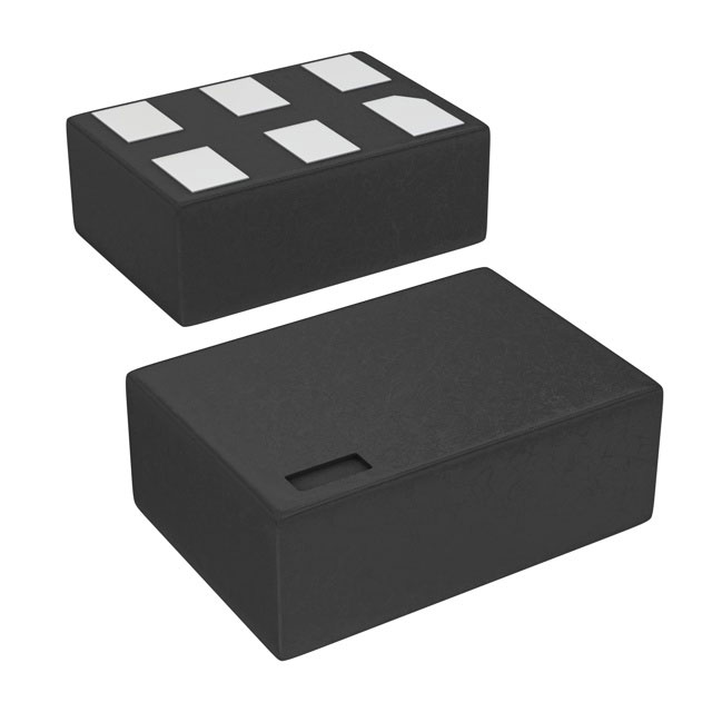
- Package: SOT-23-6
- Essence: The NC7SV125L6X is a versatile logic level shifter designed to convert signals between different voltage levels in electronic circuits.
- Packaging/Quantity: Available in tape and reel packaging with 3000 units per reel.
Specifications
The NC7SV125L6X has the following specifications:
- Supply Voltage: 1.65V to 5.5V
- Input Voltage Range: 0V to VCC
- Output Voltage Range: 0V to VCC
- Propagation Delay: 2.5ns (typical)
- Operating Temperature Range: -40°C to +85°C
Detailed Pin Configuration
The NC7SV125L6X features a 6-pin SOT-23 package with the following pin configuration:
____
   A1 |    | VCC
   A2 |    | B1
   GND |    | B2
   A3 |    | OE#
   A4 |    | B3
   A5 |____| B4
Functional Features
- Non-inverting buffer: The NC7SV125L6X provides a non-inverting buffer function, ensuring that the output signal matches the input signal polarity.
- Logic level shifting: It allows for seamless conversion of signals between different voltage levels, enabling compatibility between devices operating at different voltages.
- High-speed operation: With a propagation delay of only 2.5ns, the NC7SV125L6X ensures fast signal transmission and minimal signal distortion.
- Wide supply voltage range: The IC can operate within a wide supply voltage range of 1.65V to 5.5V, making it suitable for various applications.
Advantages and Disadvantages
Advantages:
- Compact package size
- Low-voltage operation
- High-speed performance
- Easy integration into existing circuits
- Versatile application possibilities
Disadvantages:
- Limited output current drive capability
- Not suitable for high-power applications
Working Principles
The NC7SV125L6X operates based on CMOS (Complementary Metal-Oxide-Semiconductor) technology. It utilizes a combination of NMOS and PMOS transistors to achieve logic level shifting. When the input signal is at a low voltage level, the NMOS transistor allows the signal to pass through, while blocking it when the input signal is at a high voltage level. Similarly, the PMOS transistor performs the opposite function. This mechanism ensures that the output signal matches the input signal polarity while shifting the voltage level accordingly.
Detailed Application Field Plans
The NC7SV125L6X finds applications in various fields, including but not limited to:
- Consumer Electronics: Used in smartphones, tablets, and portable devices for voltage level conversion between different components.
- Industrial Automation: Enables communication between devices operating at different voltage levels in industrial control systems.
- Automotive Electronics: Facilitates signal conversion in automotive electronic systems, such as infotainment systems and engine control units.
- IoT Devices: Allows for seamless integration of sensors and actuators operating at different voltage levels in IoT (Internet of Things) devices.
- Telecommunications: Utilized in networking equipment to convert signals between different voltage domains.
Detailed and Complete Alternative Models
- SN74LVC1T45: Single-bit dual-supply bus transceiver
- 74LVC1T125: Single-gate non-inverting buffer/line driver with 3-state output
These alternative models offer similar functionality and can be considered as alternatives to the NC7SV125L6X based on specific application requirements.
Word count: 511 words
10個與NC7SV125L6X在技術方案中應用相關的常見問題與解答
Sure! Here are 10 common questions and answers related to the application of NC7SV125L6X in technical solutions:
Question: What is the NC7SV125L6X?
Answer: The NC7SV125L6X is a quad buffer gate IC (integrated circuit) that provides high-speed signal buffering and level shifting capabilities.Question: What is the operating voltage range of the NC7SV125L6X?
Answer: The NC7SV125L6X operates within a voltage range of 1.65V to 5.5V, making it compatible with a wide range of digital systems.Question: What is the maximum data rate supported by the NC7SV125L6X?
Answer: The NC7SV125L6X supports data rates up to 400 Mbps, making it suitable for high-speed applications.Question: Can the NC7SV125L6X be used as a level shifter?
Answer: Yes, the NC7SV125L6X can be used as a level shifter to convert signals between different voltage levels, enabling compatibility between devices with different voltage requirements.Question: How many buffer gates are there in the NC7SV125L6X?
Answer: The NC7SV125L6X consists of four independent buffer gates, allowing for multiple signal buffering operations.Question: What is the typical propagation delay of the NC7SV125L6X?
Answer: The typical propagation delay of the NC7SV125L6X is around 2.5 ns, ensuring fast signal transmission.Question: Is the NC7SV125L6X suitable for battery-powered applications?
Answer: Yes, the NC7SV125L6X has a low power consumption and can be used in battery-powered applications, helping to conserve energy.Question: Can the NC7SV125L6X handle both push-pull and open-drain outputs?
Answer: Yes, the NC7SV125L6X supports both push-pull and open-drain output configurations, providing flexibility in various circuit designs.Question: What is the package type of the NC7SV125L6X?
Answer: The NC7SV125L6X is available in a small SOT-23-6 package, which is compact and suitable for space-constrained applications.Question: Are there any recommended application circuits available for the NC7SV125L6X?
Answer: Yes, the datasheet of the NC7SV125L6X provides recommended application circuits that can help users understand and implement the IC effectively in their designs.
Please note that these answers are general and may vary depending on specific design requirements and use cases. It's always recommended to refer to the datasheet and consult with technical experts for accurate information and guidance.