

Encyclopedia Entry: 74ABT899CQC
Product Overview
Category
The 74ABT899CQC belongs to the category of integrated circuits (ICs) and specifically falls under the family of ABT series ICs.
Use
This IC is primarily used for data storage and retrieval purposes in digital systems. It serves as a high-speed, 8-bit shift register with parallel input and output capabilities.
Characteristics
- High-speed operation: The 74ABT899CQC is designed to operate at high clock frequencies, making it suitable for applications requiring fast data transfer.
- Parallel input/output: It features parallel input and output ports, allowing for efficient data exchange between the IC and other components.
- Shift register functionality: The IC can store and shift data bits serially, enabling sequential data processing.
- Compatibility: The 74ABT899CQC is compatible with both TTL and CMOS logic levels, providing flexibility in system integration.
Package and Quantity
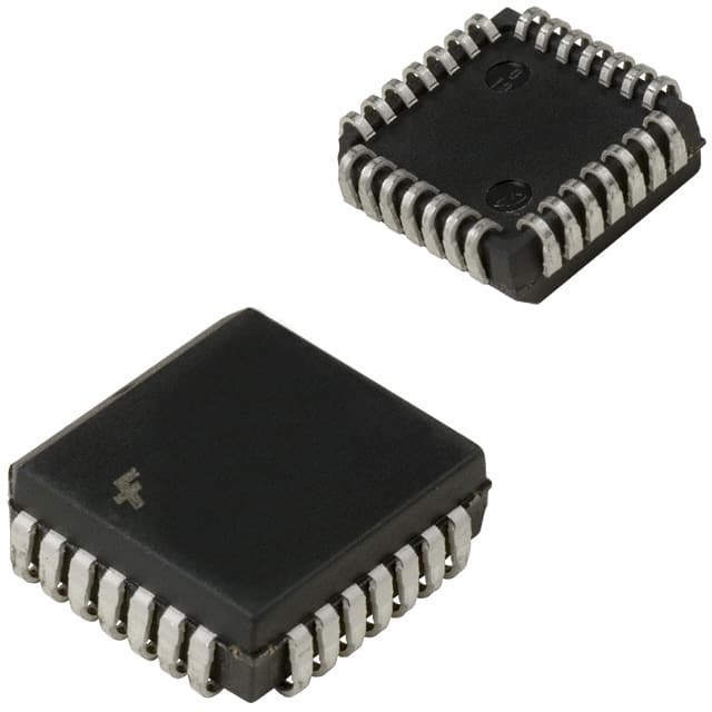
The 74ABT899CQC is available in a quad flat package (QFP), which ensures easy mounting on printed circuit boards (PCBs). It is typically sold in reels or tubes containing multiple units.
Essence
The essence of the 74ABT899CQC lies in its ability to facilitate high-speed data storage and retrieval operations within digital systems. Its parallel input/output and shift register functionality make it a versatile component for various applications.
Specifications
- Supply voltage: 4.5V to 5.5V
- Operating temperature range: -40°C to +85°C
- Input/output compatibility: TTL and CMOS
- Clock frequency: Up to 100 MHz
- Data width: 8 bits
- Package type: Quad flat package (QFP)
Pin Configuration
The 74ABT899CQC features a total of 44 pins, each serving a specific function. The detailed pin configuration is as follows:
- Pin 1: Serial Data Input (DSI)
- Pin 2: Serial Data Output (DSO)
- Pin 3: Clock Input (CLK)
- Pin 4: Parallel Data Input (D0)
- Pin 5: Parallel Data Input (D1)
- Pin 6: Parallel Data Input (D2)
- Pin 7: Parallel Data Input (D3)
- Pin 8: Parallel Data Input (D4)
- Pin 9: Parallel Data Input (D5)
- Pin 10: Parallel Data Input (D6)
- Pin 11: Parallel Data Input (D7)
- Pin 12: Enable Input (EN)
- Pin 13: Clear Input (CLR)
- Pin 14: Shift/Load Input (S/L)
- Pin 15: Serial Data Input (DSI)
- Pin 16: Serial Data Output (DSO)
- Pin 17: Clock Input (CLK)
- Pin 18: Parallel Data Output (Q0)
- Pin 19: Parallel Data Output (Q1)
- Pin 20: Parallel Data Output (Q2)
- Pin 21: Parallel Data Output (Q3)
- Pin 22: Parallel Data Output (Q4)
- Pin 23: Parallel Data Output (Q5)
- Pin 24: Parallel Data Output (Q6)
- Pin 25: Parallel Data Output (Q7)
- Pin 26: Enable Input (EN)
- Pin 27: Clear Input (CLR)
- Pin 28: Shift/Load Input (S/L) 29-44: Ground and Power Supply Pins
Functional Features
Shift Register Operation
The 74ABT899CQC can function as an 8-bit shift register. When the Shift/Load (S/L) input is low, data is shifted through the IC from the Serial Data Input (DSI) pin to the Serial Data Output (DSO) pin on each clock pulse. The parallel data inputs (D0-D7) are ignored during this operation.
Parallel Load Operation
When the S/L input is high, the IC enters the parallel load mode. In this mode, the data present at the parallel data inputs (D0-D7) is loaded into the shift register on the rising edge of the clock signal. The loaded data can then be shifted out serially or held in the shift register for further processing.
Clear Functionality
The Clear (CLR) input allows for clearing the shift register and all outputs to a low logic level when activated. This feature is useful for initializing the IC or resetting its state.
Advantages and Disadvantages
Advantages
- High-speed operation enables efficient data transfer.
- Compatibility with TTL and CMOS logic levels provides flexibility in system integration.
10個與74ABT899CQC在技術方案中應用相關的常見問題與解答
Sure! Here are 10 common questions and answers related to the application of 74ABT899CQC in technical solutions:
Q: What is the purpose of the 74ABT899CQC integrated circuit? A: The 74ABT899CQC is a high-speed, 8-bit universal shift register with parallel inputs and outputs.
Q: What is the maximum clock frequency supported by the 74ABT899CQC? A: The 74ABT899CQC can operate at a maximum clock frequency of 100 MHz.
Q: How many parallel inputs and outputs does the 74ABT899CQC have? A: The 74ABT899CQC has 8 parallel inputs and 8 parallel outputs.
Q: Can the 74ABT899CQC be used for serial-to-parallel or parallel-to-serial conversion? A: Yes, the 74ABT899CQC can be used for both serial-to-parallel and parallel-to-serial conversion.
Q: What is the power supply voltage range for the 74ABT899CQC? A: The 74ABT899CQC operates with a power supply voltage range of 4.5V to 5.5V.
Q: Does the 74ABT899CQC support tri-state outputs? A: Yes, the 74ABT899CQC supports tri-state outputs, allowing multiple devices to share a common bus.
Q: Can the 74ABT899CQC be cascaded to increase the number of bits? A: Yes, multiple 74ABT899CQC ICs can be cascaded together to increase the number of bits in the shift register.
Q: What is the typical propagation delay of the 74ABT899CQC? A: The typical propagation delay of the 74ABT899CQC is around 5 ns.
Q: Is the 74ABT899CQC compatible with TTL logic levels? A: Yes, the 74ABT899CQC is compatible with both TTL and CMOS logic levels.
Q: Can the 74ABT899CQC be used in high-speed data communication applications? A: Yes, the 74ABT899CQC is suitable for high-speed data communication applications due to its fast operation and compatibility with various logic levels.
Please note that these answers are general and may vary depending on specific application requirements and datasheet specifications.