

74LVT16244BEV,157
Basic Information Overview
- Category: Integrated Circuit (IC)
- Use: Buffer/Driver
- Characteristics: Low Voltage, 16-bit, Tri-State, Non-Inverting
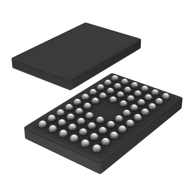
- Package: TSSOP (Thin Shrink Small Outline Package)
- Essence: High-speed CMOS buffer/driver with tri-state outputs
- Packaging/Quantity: Tape and Reel, 2500 units per reel
Specifications
- Supply Voltage Range: 2.7V to 3.6V
- Input Voltage Range: 0V to VCC
- Output Voltage Range: 0V to VCC
- Operating Temperature Range: -40°C to +85°C
- Propagation Delay Time: 4.5ns (max)
- Output Current: ±24mA
- Input Capacitance: 4pF (typ)
- Output Capacitance: 8pF (typ)
Detailed Pin Configuration
The 74LVT16244BEV,157 IC has a total of 48 pins, which are divided into two groups of 24 pins each. The pin configuration is as follows:
Group A:
- OE (Output Enable) 1
- Y1 (Output) 1
- GND (Ground)
- Y2 (Output) 1
- Y3 (Output) 1
- Y4 (Output) 1
- VCC (Supply Voltage)
- Y5 (Output) 1
- Y6 (Output) 1
- Y7 (Output) 1
- Y8 (Output) 1
- GND (Ground)
- Y9 (Output) 1
- Y10 (Output) 1
- Y11 (Output) 1
- Y12 (Output) 1
- VCC (Supply Voltage)
- Y13 (Output) 1
- Y14 (Output) 1
- Y15 (Output) 1
- Y16 (Output) 1
- GND (Ground)
- Y17 (Output) 1
- Y18 (Output) 1
Group B:
- OE (Output Enable) 2
- Y1 (Output) 2
- GND (Ground)
- Y2 (Output) 2
- Y3 (Output) 2
- Y4 (Output) 2
- VCC (Supply Voltage)
- Y5 (Output) 2
- Y6 (Output) 2
- Y7 (Output) 2
- Y8 (Output) 2
- GND (Ground)
- Y9 (Output) 2
- Y10 (Output) 2
- Y11 (Output) 2
- Y12 (Output) 2
- VCC (Supply Voltage)
- Y13 (Output) 2
- Y14 (Output) 2
- Y15 (Output) 2
- Y16 (Output) 2
- GND (Ground)
- Y17 (Output) 2
- Y18 (Output) 2
Functional Features
- High-speed operation: The 74LVT16244BEV,157 is designed to operate at high speeds, making it suitable for applications requiring fast data transmission.
- Tri-state outputs: The IC has tri-state outputs, allowing multiple devices to share a common bus without interfering with each other.
- Non-inverting: The buffer/driver does not invert the input signal, maintaining its original logic level at the output.
Advantages and Disadvantages
Advantages:
- High-speed operation enables efficient data transmission.
- Tri-state outputs facilitate bus sharing in multi-device systems.
- Non-inverting nature preserves the logic level of the input signal.
Disadvantages:
- Limited supply voltage range (2.7V to 3.6V) may restrict compatibility with certain systems.
- Propagation delay time of 4.5ns (max) may introduce slight delays in critical applications.
Working Principles
The 74LVT16244BEV,157 is a CMOS buffer/driver that amplifies and buffers digital signals. It operates by receiving an input signal and providing a corresponding amplified output signal. The tri-state outputs allow the IC to be connected to a common bus, where it can either drive the bus with its output or enter a high-impedance state, effectively disconnecting from the bus.
Detailed Application Field Plans
The 74LVT16244BEV,157 is commonly used
10個與74LVT16244BEV,157在技術方案中應用相關的常見問題與解答
Sure! Here are 10 common questions and answers related to the application of 74LVT16244BEV,157 in technical solutions:
Q: What is the function of the 74LVT16244BEV,157? A: The 74LVT16244BEV,157 is a 16-bit buffer/driver with 3-state outputs. It is used to amplify and control signals in digital circuits.
Q: What is the maximum operating voltage for the 74LVT16244BEV,157? A: The maximum operating voltage for the 74LVT16244BEV,157 is typically 3.3V.
Q: Can the 74LVT16244BEV,157 be used with both TTL and CMOS logic levels? A: Yes, the 74LVT16244BEV,157 is compatible with both TTL and CMOS logic levels.
Q: What is the output current capability of the 74LVT16244BEV,157? A: The 74LVT16244BEV,157 has a typical output current capability of ±32mA.
Q: How many 74LVT16244BEV,157 devices can be connected together in a single circuit? A: Multiple 74LVT16244BEV,157 devices can be connected together in a circuit, as long as the total output current does not exceed the specified limits.
Q: Does the 74LVT16244BEV,157 have built-in protection against electrostatic discharge (ESD)? A: Yes, the 74LVT16244BEV,157 has built-in ESD protection to prevent damage from static electricity.
Q: Can the 74LVT16244BEV,157 be used in high-speed applications? A: Yes, the 74LVT16244BEV,157 is designed for high-speed operation and can be used in applications with fast switching requirements.
Q: What is the power supply voltage range for the 74LVT16244BEV,157? A: The power supply voltage range for the 74LVT16244BEV,157 is typically between 2.7V and 3.6V.
Q: Does the 74LVT16244BEV,157 have internal pull-up or pull-down resistors? A: No, the 74LVT16244BEV,157 does not have internal pull-up or pull-down resistors. External resistors may be required for specific applications.
Q: Is the 74LVT16244BEV,157 available in different package options? A: Yes, the 74LVT16244BEV,157 is available in various package options, such as SOIC, TSSOP, and SSOP, to accommodate different circuit designs and assembly methods.
Please note that the answers provided here are general and may vary depending on the specific datasheet and manufacturer's specifications for the 74LVT16244BEV,157.