

74HC2G126DC,125
Basic Information Overview
- Category: Integrated Circuit (IC)
- Use: Logic Gate Buffer/Driver
- Characteristics: High-Speed, Low-Power, Dual Bus Buffer
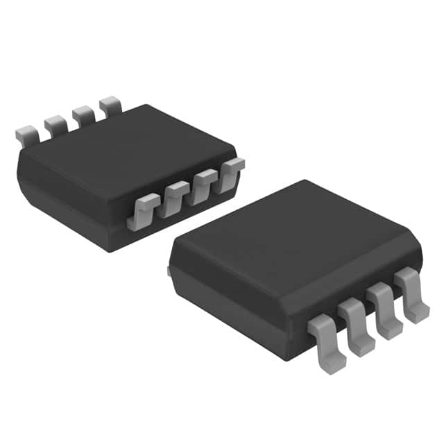
- Package: 8-pin SOIC (Small Outline Integrated Circuit)
- Essence: Buffering and driving signals in digital circuits
- Packaging/Quantity: Tape and Reel, 2500 units per reel
Specifications
- Supply Voltage Range: 2V to 6V
- Input Voltage Range: 0V to VCC
- Output Voltage Range: 0V to VCC
- Maximum Operating Frequency: 400 MHz
- Propagation Delay: 4.5 ns (typical)
- Output Current: ±8 mA
- Operating Temperature Range: -40°C to +85°C
Detailed Pin Configuration
- GND (Ground)
- A (Input A)
- B (Input B)
- OE (Output Enable)
- Y (Output Y)
- NC (No Connection)
- VCC (Supply Voltage)
- GND (Ground)
Functional Features
- Dual Buffer: Can buffer two independent input signals
- High-Speed Operation: Suitable for high-frequency applications
- Low Power Consumption: Helps reduce overall power consumption in circuits
- Wide Supply Voltage Range: Allows flexibility in different voltage systems
- Output Enable Function: Enables or disables the output signal
Advantages
- Compact Size: The 8-pin SOIC package offers a small footprint
- Versatile: Can be used in various digital circuit applications
- Reliable Performance: Manufactured using advanced semiconductor technology
- Cost-Effective: Provides a cost-effective solution for buffering signals
Disadvantages
- Limited Output Current: May not be suitable for driving heavy loads
- Sensitivity to Noise: High-speed operation makes it susceptible to noise interference
- Limited Temperature Range: Operating temperature range is limited to -40°C to +85°C
Working Principles
The 74HC2G126DC,125 is a dual buffer IC that operates as a voltage level translator and signal driver. It takes two independent input signals (A and B) and buffers them to provide amplified and synchronized output signals (Y). The output enable (OE) pin controls the activation of the buffer, allowing the user to enable or disable the output signal.
Detailed Application Field Plans
- Digital Communication Systems
- Microcontrollers and Microprocessors
- Data Storage Devices
- Industrial Automation Systems
- Consumer Electronics
Detailed and Complete Alternative Models
- SN74LVC2G126DCURG4
- MC74VHC1G126DFT1G
- TC7SZ126AFK(TE12L,Q)
(Note: These alternative models may have slightly different specifications and pin configurations but serve similar functions.)
This entry provides an overview of the 74HC2G126DC,125 integrated circuit, including its basic information, specifications, pin configuration, functional features, advantages, disadvantages, working principles, application field plans, and alternative models.
10個與74HC2G126DC,125在技術方案中應用相關的常見問題與解答
Sure! Here are 10 common questions and answers related to the application of 74HC2G126DC,125 in technical solutions:
Q: What is the function of the 74HC2G126DC,125? A: The 74HC2G126DC,125 is a dual bus buffer gate with 3-state outputs. It can be used for signal buffering and level shifting.
Q: What is the operating voltage range of the 74HC2G126DC,125? A: The operating voltage range is typically between 2V and 6V.
Q: Can the 74HC2G126DC,125 handle high-speed signals? A: Yes, it has a high-speed CMOS technology that allows it to handle fast switching signals.
Q: How many inputs and outputs does the 74HC2G126DC,125 have? A: It has two inputs and two outputs.
Q: What is the maximum output current of the 74HC2G126DC,125? A: The maximum output current is typically around 8mA.
Q: Can I use the 74HC2G126DC,125 for level shifting between different voltage domains? A: Yes, it can be used for level shifting as long as the voltage levels are within its operating range.
Q: Does the 74HC2G126DC,125 have internal pull-up or pull-down resistors? A: No, it does not have internal pull-up or pull-down resistors. External resistors may be required if needed.
Q: Can I connect multiple 74HC2G126DC,125 devices together to increase the number of inputs/outputs? A: Yes, multiple devices can be connected together to increase the number of inputs/outputs.
Q: What is the power supply current consumption of the 74HC2G126DC,125? A: The power supply current consumption is typically very low, around a few microamps.
Q: Can I use the 74HC2G126DC,125 in battery-powered applications? A: Yes, its low power consumption makes it suitable for battery-powered applications.
Please note that the answers provided are general and may vary depending on specific datasheet specifications and application requirements.