

Encyclopedia Entry: 74ABT657DB,112
Product Overview
Category
The 74ABT657DB,112 belongs to the category of integrated circuits (ICs) and specifically falls under the family of digital logic ICs.
Use
This product is primarily used for data bus multiplexing and demultiplexing applications in various electronic devices and systems.
Characteristics
- High-speed operation
- Low power consumption
- Wide operating voltage range
- Schmitt-trigger inputs for noise immunity
- Output capability: balanced propagation delays and transition times
Package
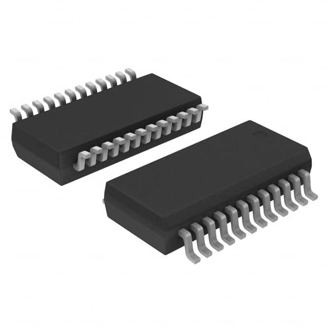
The 74ABT657DB,112 is available in a standard 24-pin SSOP (Shrink Small Outline Package) package.
Essence
The essence of this product lies in its ability to efficiently handle data bus multiplexing and demultiplexing tasks, enabling effective data transmission and control within electronic systems.
Packaging/Quantity
The 74ABT657DB,112 is typically packaged in reels or tubes, with a quantity of 250 units per reel/tube.
Specifications
- Supply Voltage Range: 4.5V to 5.5V
- Input Voltage Range: 0V to VCC
- Operating Temperature Range: -40°C to +85°C
- Maximum Propagation Delay: 7 ns
- Maximum Input Capacitance: 10 pF
- Maximum Output Current: ±32 mA
Detailed Pin Configuration
The 74ABT657DB,112 has a total of 24 pins, each serving a specific function. The pin configuration is as follows:
- A0 (Input)
- A1 (Input)
- A2 (Input)
- A3 (Input)
- A4 (Input)
- A5 (Input)
- A6 (Input)
- A7 (Input)
- OE (Output Enable, Input)
- SEL (Select, Input)
- B0 (Input/Output)
- B1 (Input/Output)
- B2 (Input/Output)
- B3 (Input/Output)
- B4 (Input/Output)
- B5 (Input/Output)
- B6 (Input/Output)
- B7 (Input/Output)
- GND (Ground)
- VCC (Power Supply)
- C0 (Output)
- C1 (Output)
- C2 (Output)
- C3 (Output)
Functional Features
The 74ABT657DB,112 offers the following functional features:
- Data bus multiplexing and demultiplexing
- Output enable control for data transmission control
- Select input for choosing between multiplexing and demultiplexing modes
- High-speed operation for efficient data handling
- Schmitt-trigger inputs for improved noise immunity
Advantages and Disadvantages
Advantages
- High-speed operation allows for quick data transmission.
- Low power consumption helps in energy-efficient designs.
- Wide operating voltage range provides flexibility in various applications.
- Schmitt-trigger inputs enhance noise immunity, ensuring reliable data handling.
Disadvantages
- Limited number of data lines (8) may restrict its use in applications requiring a higher number of data channels.
- The SSOP package may not be suitable for all PCB layouts or assembly processes.
Working Principles
The 74ABT657DB,112 operates based on the principles of digital logic. It utilizes multiplexers and demultiplexers to efficiently route data between different sources and destinations. The select input determines whether the device functions as a multiplexer or a demultiplexer. When used as a multiplexer, it combines multiple input signals into a single output line. In demultiplexer mode, it distributes a single input signal to multiple output lines.
Detailed Application Field Plans
The 74ABT657DB,112 finds applications in various electronic systems that require data bus multiplexing and demultiplexing capabilities. Some specific application fields include:
- Communication Systems: Used for efficient data routing in communication networks and protocols.
- Industrial Automation: Enables effective control and monitoring of data buses in industrial automation systems.
- Automotive Electronics: Facilitates data transmission and control in automotive electronics, such as infotainment systems and vehicle diagnostics.
- Computer Peripherals: Utilized in devices like printers, scanners, and external storage systems for data handling and control.
Detailed and Complete Alternative Models
There are several alternative models available in the market that offer similar functionality to the 74ABT657DB,112. Some notable alternatives include:
- 74HC257: A CMOS-based quad 2-input multiplexer/demultiplexer IC.
- CD4051B: An analog multiplexer/demultiplexer IC with 8 channels.
- SN74LS151
10個與74ABT657DB,112在技術方案中應用相關的常見問題與解答
Sure! Here are 10 common questions and answers related to the application of 74ABT657DB,112 in technical solutions:
1. What is the function of the 74ABT657DB,112? The 74ABT657DB,112 is an octal transceiver with parity generator/checker.
2. How many data inputs does the 74ABT657DB,112 have? The 74ABT657DB,112 has eight data inputs (D0-D7).
3. What is the purpose of the parity generator/checker in this device? The parity generator/checker in the 74ABT657DB,112 is used to generate or check parity for the transmitted data.
4. How many control inputs does the 74ABT657DB,112 have? The 74ABT657DB,112 has three control inputs: OE (Output Enable), DIR (Direction), and P (Parity Enable).
5. What is the role of the OE (Output Enable) input? The OE input controls the output buffers of the 74ABT657DB,112. When OE is low, the outputs are enabled; when OE is high, the outputs are disabled.
6. How does the DIR (Direction) input affect the operation of the 74ABT657DB,112? The DIR input determines the direction of data flow. When DIR is low, data is transmitted from A to B; when DIR is high, data is transmitted from B to A.
7. Can the 74ABT657DB,112 operate with different supply voltages? Yes, the 74ABT657DB,112 is designed to work with a wide range of supply voltages, typically between 4.5V and 5.5V.
8. What is the maximum data rate supported by the 74ABT657DB,112? The 74ABT657DB,112 can support a maximum data rate of 200 MHz.
9. How does the P (Parity Enable) input affect the parity generation/checking? When the P input is low, the device operates in parity generator mode, generating the parity bit based on the data inputs. When P is high, it operates in parity checker mode, checking the received data for parity errors.
10. Can the 74ABT657DB,112 be cascaded with other similar devices? Yes, multiple 74ABT657DB,112 devices can be cascaded together to increase the number of data inputs/outputs or to implement more complex data transmission systems.
Please note that the answers provided here are general and may vary depending on the specific application and requirements.