

74LVTH244ABQ,115
Basic Information Overview
- Category: Integrated Circuit (IC)
- Use: Buffer/Line Driver
- Characteristics: High-speed, low-power, voltage-level translation
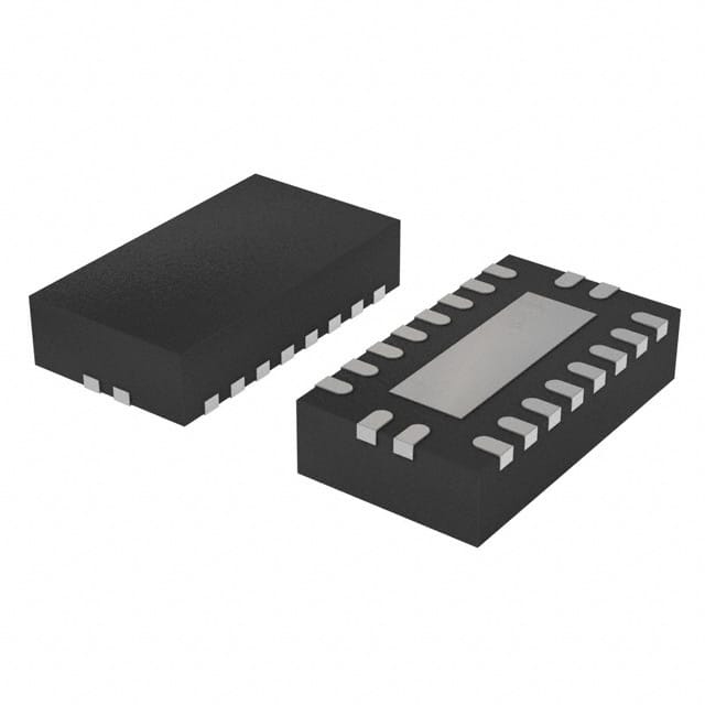
- Package: TSSOP (Thin Shrink Small Outline Package)
- Essence: Logic Level Translator
- Packaging/Quantity: Tape and Reel, 2500 units per reel
Specifications
- Supply Voltage Range: 1.2V to 3.6V
- Input Voltage Range: 0V to VCC
- Output Voltage Range: 0V to VCC
- Maximum Operating Frequency: 180MHz
- Number of Channels: 8
- Input/Output Type: Non-Inverting
- Propagation Delay Time: 4.5ns (max) at 3.3V supply
- Output Drive Capability: ±24mA
Detailed Pin Configuration
The 74LVTH244ABQ,115 IC has a total of 20 pins, which are assigned as follows:
- Pin 1: Output 1 (Y1)
- Pin 2: Output 2 (Y2)
- Pin 3: Output 3 (Y3)
- Pin 4: Output 4 (Y4)
- Pin 5: GND (Ground)
- Pin 6: Input 4 (A4)
- Pin 7: Input 3 (A3)
- Pin 8: Input 2 (A2)
- Pin 9: Input 1 (A1)
- Pin 10: VCC (Supply Voltage)
- Pin 11: Enable (EN)
- Pin 12: Output 5 (Y5)
- Pin 13: Output 6 (Y6)
- Pin 14: Output 7 (Y7)
- Pin 15: Output 8 (Y8)
- Pin 16: GND (Ground)
- Pin 17: Input 8 (A8)
- Pin 18: Input 7 (A7)
- Pin 19: Input 6 (A6)
- Pin 20: Input 5 (A5)
Functional Features
- Voltage-level translation between different logic levels
- Non-inverting buffer/line driver
- High-speed operation with low power consumption
- Wide supply voltage range for compatibility with various systems
- 3-state outputs for bus-oriented applications
- Schmitt-trigger inputs for noise immunity
Advantages and Disadvantages
Advantages: - High-speed operation allows for efficient data transfer - Low-power consumption helps in reducing overall system energy usage - Wide supply voltage range enables compatibility with different devices - 3-state outputs facilitate bus sharing and multiplexing - Schmitt-trigger inputs provide noise immunity, ensuring reliable operation
Disadvantages: - Limited output drive capability may restrict use in high-current applications - TSSOP package may require careful handling during assembly and soldering
Working Principles
The 74LVTH244ABQ,115 is a logic level translator that operates by receiving input signals at one voltage level and providing corresponding output signals at a different voltage level. It utilizes a combination of CMOS and TTL technologies to achieve high-speed operation with low power consumption. The IC incorporates Schmitt-trigger inputs, which help in reducing the effects of noise and ensuring reliable signal reception. The 3-state outputs allow multiple devices to share a common bus, enabling efficient communication between different components.
Detailed Application Field Plans
The 74LVTH244ABQ,115 IC finds applications in various fields where voltage-level translation and buffering are required. Some potential application areas include: - Microcontroller interfacing - Memory address decoding - Data communication systems - Industrial automation - Automotive electronics - Consumer electronics
Detailed and Complete Alternative Models
- 74LVTH244A: Similar functionality with different package options (SOIC, TSSOP, SSOP)
- 74LVC244A: Lower voltage operation (1.2V to 3.6V) with similar characteristics
- SN74LVTH244A: Equivalent IC from Texas Instruments with comparable specifications
(Note: The above alternative models are provided as examples and may not cover all available alternatives in the market.)
This encyclopedia entry provides a comprehensive overview of the 74LVTH244ABQ,115 IC, including its basic information, specifications, pin configuration, functional features, advantages and disadvantages, working principles, application field plans, and alternative models.
10個與74LVTH244ABQ,115在技術方案中應用相關的常見問題與解答
Sure! Here are 10 common questions and answers related to the application of 74LVTH244ABQ,115 in technical solutions:
Q: What is the function of the 74LVTH244ABQ,115? A: The 74LVTH244ABQ,115 is an octal buffer/line driver with 3-state outputs.
Q: What is the voltage supply range for this IC? A: The voltage supply range for the 74LVTH244ABQ,115 is typically between 2.7V and 3.6V.
Q: How many input/output pins does it have? A: The 74LVTH244ABQ,115 has 8 input pins and 8 output pins.
Q: Can I use this IC for level shifting applications? A: Yes, the 74LVTH244ABQ,115 can be used for level shifting as it supports both TTL and CMOS voltage levels.
Q: What is the maximum output current it can drive? A: The 74LVTH244ABQ,115 can drive up to 32mA of output current per channel.
Q: Is this IC suitable for high-speed applications? A: Yes, the 74LVTH244ABQ,115 is designed for high-speed operation and has a propagation delay of only a few nanoseconds.
Q: Can I connect multiple ICs together to increase the number of channels? A: Yes, you can connect multiple 74LVTH244ABQ,115 ICs together to increase the number of channels by cascading them.
Q: Does this IC have built-in protection features? A: Yes, the 74LVTH244ABQ,115 has built-in ESD protection on all inputs and outputs.
Q: Can I use this IC in automotive applications? A: Yes, the 74LVTH244ABQ,115 is qualified for automotive applications and meets the necessary standards.
Q: What is the package type for this IC? A: The 74LVTH244ABQ,115 is available in a standard SOIC-20 package.
Please note that these answers are general and may vary depending on specific datasheet specifications and application requirements.