

Encyclopedia Entry: 74AHCT1G04GV,125
Product Information Overview
Category: Integrated Circuit (IC)
Use: The 74AHCT1G04GV,125 is a single inverter gate IC that is commonly used in digital logic circuits. It is designed to convert input signals into their complementary form.
Characteristics: - High-speed operation - Low power consumption - Wide operating voltage range - Schmitt-trigger action for noise immunity
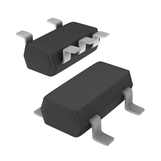
Package: SOT-23-5 package
Essence: The essence of the 74AHCT1G04GV,125 lies in its ability to perform logical inversion, making it an essential component in various digital systems.
Packaging/Quantity: The 74AHCT1G04GV,125 is typically available in reels containing 3000 units.
Specifications
- Supply Voltage Range: 4.5V to 5.5V
- Input Voltage Range: 0V to VCC
- Output Voltage Range: 0V to VCC
- Operating Temperature Range: -40°C to +85°C
- Propagation Delay Time: 6 ns (max)
- Output Current: ±8 mA
Detailed Pin Configuration
The 74AHCT1G04GV,125 has a total of 5 pins:
- GND (Ground): Connected to the ground reference of the circuit.
- A (Input): Accepts the input signal to be inverted.
- Y (Output): Provides the inverted output signal.
- NC (No Connection): This pin is not connected and should be left unconnected.
- VCC (Power Supply): Connected to the positive supply voltage.
Functional Features
- Logical Inversion: The 74AHCT1G04GV,125 performs the function of logical inversion, where the output is the complement of the input signal.
- Schmitt-trigger Action: The IC incorporates a Schmitt-trigger action, which ensures noise immunity and stable output even in the presence of input signal fluctuations.
- High-Speed Operation: With a propagation delay time of only 6 ns, the IC enables fast switching between logic levels.
- Low Power Consumption: The IC is designed to consume minimal power, making it suitable for battery-powered applications.
Advantages and Disadvantages
Advantages: - Compact Size: The SOT-23-5 package allows for space-efficient integration into electronic circuits. - Wide Operating Voltage Range: The IC can operate within a wide range of supply voltages, providing flexibility in various applications. - Noise Immunity: The Schmitt-trigger action enhances the IC's ability to reject noise and maintain stable output signals.
Disadvantages: - Single Functionality: The IC only performs logical inversion and does not offer additional functions like other complex logic gates. - Limited Output Current: The maximum output current of ±8 mA may restrict its use in applications requiring higher current drive capabilities.
Working Principles
The 74AHCT1G04GV,125 operates based on the principles of complementary metal-oxide-semiconductor (CMOS) technology. It utilizes a combination of NMOS and PMOS transistors to achieve logical inversion. When the input signal is high, the NMOS transistor conducts, pulling the output voltage low. Conversely, when the input signal is low, the PMOS transistor conducts, driving the output voltage high.
Detailed Application Field Plans
The 74AHCT1G04GV,125 finds application in various digital systems and electronic devices, including but not limited to: - Microcontrollers - Digital signal processing circuits - Communication systems - Consumer electronics - Industrial automation
Detailed and Complete Alternative Models
Some alternative models that serve similar functions to the 74AHCT1G04GV,125 include: - SN74AHC1G04DBVR - MC74VHC1G04DTT1G - TC7SZ04FU
These alternative models offer comparable features and can be used as substitutes depending on specific application requirements.
Word Count: 498 words
10個與74AHCT1G04GV,125在技術方案中應用相關的常見問題與解答
Sure! Here are 10 common questions and answers related to the application of 74AHCT1G04GV,125 in technical solutions:
Q1: What is the 74AHCT1G04GV,125? A1: The 74AHCT1G04GV,125 is a single inverter gate IC (Integrated Circuit) that is commonly used in digital logic circuits.
Q2: What is the voltage supply range for the 74AHCT1G04GV,125? A2: The voltage supply range for the 74AHCT1G04GV,125 is typically between 4.5V and 5.5V.
Q3: What is the maximum output current of the 74AHCT1G04GV,125? A3: The maximum output current of the 74AHCT1G04GV,125 is around 8mA.
Q4: Can the 74AHCT1G04GV,125 be used as a level shifter? A4: Yes, the 74AHCT1G04GV,125 can be used as a level shifter to convert signals from one voltage level to another.
Q5: What is the propagation delay of the 74AHCT1G04GV,125? A5: The propagation delay of the 74AHCT1G04GV,125 is typically around 6 ns.
Q6: Is the 74AHCT1G04GV,125 compatible with TTL (Transistor-Transistor Logic) inputs? A6: Yes, the 74AHCT1G04GV,125 is compatible with TTL inputs and can be used as a drop-in replacement for TTL inverters.
Q7: Can the 74AHCT1G04GV,125 drive capacitive loads? A7: Yes, the 74AHCT1G04GV,125 can drive small capacitive loads without any additional buffering.
Q8: What is the operating temperature range for the 74AHCT1G04GV,125? A8: The operating temperature range for the 74AHCT1G04GV,125 is typically between -40°C and 85°C.
Q9: Can the 74AHCT1G04GV,125 be used in battery-powered applications? A9: Yes, the 74AHCT1G04GV,125 can be used in battery-powered applications as it operates at low power consumption.
Q10: Is the 74AHCT1G04GV,125 available in different package options? A10: Yes, the 74AHCT1G04GV,125 is available in various package options such as SOT23, SC-70, and XSON.