

M2S050-1FG896
Product Overview
Category
M2S050-1FG896 belongs to the category of Field Programmable Gate Arrays (FPGAs).
Use
This product is primarily used in digital logic circuits for various applications such as data processing, signal processing, and control systems.
Characteristics
- High flexibility: FPGAs can be reprogrammed to perform different functions, making them versatile for a wide range of applications.
- High performance: M2S050-1FG896 offers high-speed data processing capabilities, enabling efficient execution of complex algorithms.
- Low power consumption: This FPGA model is designed to minimize power consumption, making it suitable for battery-powered devices.
- Scalability: The M2S050-1FG896 can be easily integrated into larger systems due to its scalable architecture.
Package and Quantity
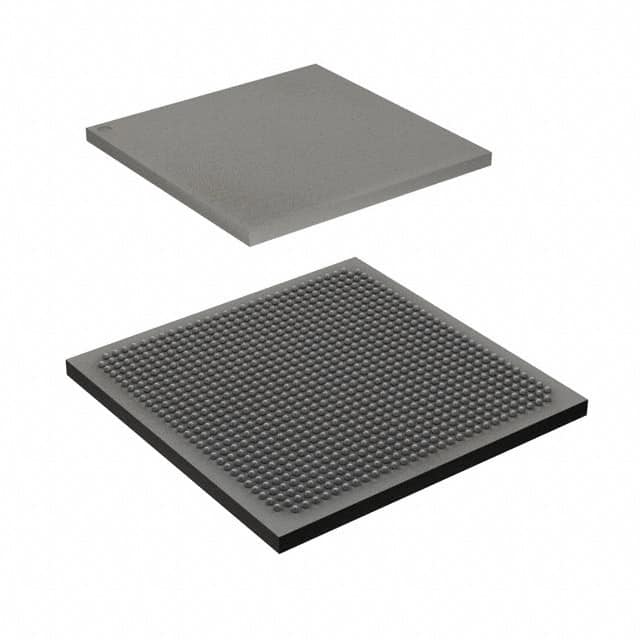
The M2S050-1FG896 comes in a compact package, measuring 17mm x 17mm. Each package contains one unit of the FPGA.
Specifications
- Model: M2S050-1FG896
- Logic Cells: 50,000
- Embedded Memory: 1,152 Kbits
- Maximum Operating Frequency: 500 MHz
- I/O Pins: 896
- Voltage Range: 1.2V - 3.3V
- Package Type: Fine-pitch Ball Grid Array (FBGA)
Pin Configuration
The detailed pin configuration of the M2S050-1FG896 can be found in the product datasheet provided by the manufacturer.
Functional Features
- Configurable Logic Blocks (CLBs): These blocks allow users to implement custom logic functions based on their specific requirements.
- Digital Signal Processing (DSP) Blocks: The FPGA includes dedicated DSP blocks that enable efficient implementation of mathematical operations.
- Input/Output (I/O) Interfaces: The M2S050-1FG896 offers a wide range of I/O interfaces, including GPIO, UART, SPI, and I2C, facilitating seamless integration with external devices.
- Clock Management: The FPGA provides various clock management resources, such as phase-locked loops (PLLs) and delay-locked loops (DLLs), ensuring precise timing control.
Advantages
- Flexibility: The reprogrammable nature of FPGAs allows for quick prototyping and design iterations.
- High Performance: The M2S050-1FG896 offers fast data processing capabilities, making it suitable for demanding applications.
- Low Power Consumption: The optimized power consumption of this FPGA model extends battery life in portable devices.
- Scalability: The FPGA's scalable architecture enables easy integration into complex systems.
Disadvantages
- Complexity: Utilizing FPGAs requires expertise in digital logic design and programming languages specific to FPGAs.
- Cost: FPGAs can be more expensive compared to other integrated circuits due to their versatility and programmability.
Working Principles
FPGAs consist of an array of configurable logic blocks interconnected through programmable routing resources. These logic blocks can be programmed to implement desired logic functions using Hardware Description Languages (HDLs) like VHDL or Verilog. Upon configuration, the FPGA operates based on the programmed logic, allowing for the execution of complex algorithms and data processing tasks.
Application Field Plans
The M2S050-1FG896 FPGA finds applications in various fields, including: - Communications: Used in wireless communication systems, network routers, and base stations. - Industrial Automation: Employed in control systems, robotics, and factory automation. - Automotive: Integrated into advanced driver-assistance systems (ADAS) and infotainment systems. - Aerospace: Utilized in satellite communication systems and flight control systems. - Medical: Applied in medical imaging devices, patient monitoring systems, and laboratory equipment.
Alternative Models
- M2S010-1FG484: A lower-capacity FPGA with 10,000 logic cells and 484 I/O pins.
- M2S150-1FGG484: A higher-capacity FPGA with 150,000 logic cells and 484 I/O pins.
- M2S250-1FGG896: A higher-capacity FPGA with 250,000 logic cells and 896 I/O pins.
These alternative models provide different capacity options to cater to varying project requirements.
In conclusion, the M2S050-1FG896 FPGA offers high flexibility, performance, and low power consumption. Its wide range of applications, along with alternative models, make it a versatile choice for digital logic circuit design.
Word Count: 529
10個與M2S050-1FG896在技術方案中應用相關的常見問題與解答
Sure! Here are 10 common questions and answers related to the application of M2S050-1FG896 in technical solutions:
Q1: What is M2S050-1FG896? A1: M2S050-1FG896 is a specific model of field-programmable gate array (FPGA) manufactured by Microsemi. It is designed for various applications in technical solutions.
Q2: What are the key features of M2S050-1FG896? A2: Some key features of M2S050-1FG896 include 50,000 logic elements, 1,152 Kbits of embedded memory, 4 PLLs, and support for various I/O standards.
Q3: What are the typical applications of M2S050-1FG896? A3: M2S050-1FG896 can be used in a wide range of applications such as industrial automation, telecommunications, automotive systems, medical devices, and more.
Q4: How can I program M2S050-1FG896? A4: M2S050-1FG896 can be programmed using industry-standard hardware description languages (HDL) like VHDL or Verilog. You can use development tools provided by Microsemi to write, compile, and program the FPGA.
Q5: Can M2S050-1FG896 interface with other components or devices? A5: Yes, M2S050-1FG896 supports various communication protocols and interfaces such as UART, SPI, I2C, Ethernet, and more. It can easily interface with other components or devices in your technical solution.
Q6: What kind of power supply does M2S050-1FG896 require? A6: M2S050-1FG896 requires a single power supply voltage of 1.2V for core logic and 3.3V for I/O banks.
Q7: Can M2S050-1FG896 be used in safety-critical applications? A7: Yes, M2S050-1FG896 is designed to meet various safety standards and can be used in safety-critical applications with proper design considerations and validation.
Q8: Does M2S050-1FG896 support encryption or security features? A8: Yes, M2S050-1FG896 provides built-in security features like bitstream encryption, tamper detection, and secure boot capabilities to protect your designs from unauthorized access or tampering.
Q9: What kind of development tools are available for M2S050-1FG896? A9: Microsemi provides Libero SoC Design Suite, which includes software tools for designing, simulating, synthesizing, and programming M2S050-1FG896. Additionally, third-party tools like Xilinx Vivado can also be used.
Q10: Where can I find more information about M2S050-1FG896? A10: You can find more detailed information about M2S050-1FG896, including datasheets, application notes, and user guides on the official Microsemi website or by contacting their technical support team.