

M2S010-1VFG400
Product Overview
Category
M2S010-1VFG400 belongs to the category of Field Programmable Gate Arrays (FPGAs).
Use
This FPGA is designed for various digital applications that require high-performance and flexible programmability.
Characteristics
- High-performance: The M2S010-1VFG400 offers fast processing speeds and efficient data handling capabilities.
- Flexibility: It allows users to reprogram the logic functions, making it adaptable to different application requirements.
- Versatility: The FPGA can be used in a wide range of industries, including telecommunications, automotive, aerospace, and consumer electronics.
Package
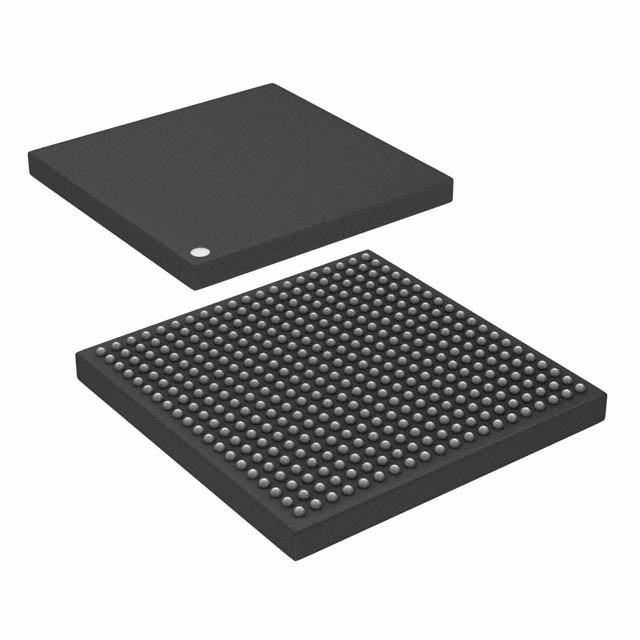
The M2S010-1VFG400 comes in a compact and durable package, ensuring easy integration into electronic systems.
Essence
The essence of this FPGA lies in its ability to provide a customizable hardware platform that enables the implementation of complex digital designs.
Packaging/Quantity
Each package contains one M2S010-1VFG400 FPGA.
Specifications
- Model: M2S010-1VFG400
- Logic Elements: 10,000
- Block RAM: 360 Kbits
- DSP Blocks: 40
- Maximum Frequency: 400 MHz
- I/O Pins: 400
- Operating Voltage: 1.2V
Detailed Pin Configuration
The M2S010-1VFG400 has a total of 400 I/O pins, which are configurable based on the specific application requirements. The pin configuration provides flexibility in connecting external devices and peripherals to the FPGA.
For a detailed pin configuration diagram, please refer to the product datasheet.
Functional Features
- High-speed data processing: The FPGA offers fast data processing capabilities, making it suitable for real-time applications.
- Reconfigurability: Users can modify the logic functions and connections within the FPGA, allowing for easy adaptation to changing requirements.
- Embedded memory: The M2S010-1VFG400 includes a substantial amount of block RAM, enabling efficient data storage and retrieval.
- DSP capabilities: With 40 dedicated DSP blocks, this FPGA can efficiently perform complex mathematical operations.
Advantages and Disadvantages
Advantages
- High performance and processing speed
- Flexibility in design and reconfiguration
- Versatile application possibilities
- Ample embedded memory for data storage
- Dedicated DSP blocks for efficient mathematical operations
Disadvantages
- Relatively higher power consumption compared to other programmable logic devices
- Steeper learning curve for beginners due to its complexity
Working Principles
The M2S010-1VFG400 operates based on the principles of digital logic. It consists of configurable logic blocks (CLBs), interconnects, and I/O elements. The CLBs contain look-up tables (LUTs) that can be programmed to implement desired logic functions. The interconnects allow for the routing of signals between different CLBs and I/O elements. By configuring the LUTs and interconnects, users can define the behavior and functionality of the FPGA.
Detailed Application Field Plans
The M2S010-1VFG400 finds applications in various fields, including:
- Telecommunications: Used in network routers, switches, and base stations for high-speed data processing and protocol handling.
- Automotive: Employed in advanced driver-assistance systems (ADAS) for real-time image processing and sensor fusion.
- Aerospace: Utilized in satellite communication systems for signal processing and control functions.
- Consumer Electronics: Integrated into smart TVs, gaming consoles, and multimedia devices for enhanced graphics and video processing.
Detailed and Complete Alternative Models
- M2S050-1VFG484: A higher-capacity FPGA with 50,000 logic elements and 484 I/O pins.
- M2S025-1VFG400: A lower-capacity FPGA with 25,000 logic elements but the same pin configuration as M2S010-1VFG400.
- M2S150-1VFG676: A higher-performance FPGA with 150,000 logic elements and 676 I/O pins.
These alternative models provide options for different project requirements, offering varying levels of logic capacity and I/O capabilities.
In conclusion, the M2S010-1VFG400 is a versatile FPGA that combines high performance, flexibility, and reconfigurability. Its applications span across multiple industries, making it a valuable component in various digital systems.
10個與M2S010-1VFG400在技術方案中應用相關的常見問題與解答
Sure! Here are 10 common questions and answers related to the application of M2S010-1VFG400 in technical solutions:
Q1: What is M2S010-1VFG400? A1: M2S010-1VFG400 is a specific model of field-programmable gate array (FPGA) manufactured by Microsemi. It is designed for various applications in embedded systems, industrial automation, and other technical solutions.
Q2: What are the key features of M2S010-1VFG400? A2: Some key features of M2S010-1VFG400 include 10,000 logic elements, 500 Kbits of embedded memory, 166 MHz maximum operating frequency, and support for various I/O standards.
Q3: What are the typical applications of M2S010-1VFG400? A3: M2S010-1VFG400 can be used in a wide range of applications such as motor control, sensor interfacing, data acquisition, communication protocols, image processing, and many more.
Q4: How do I program M2S010-1VFG400? A4: M2S010-1VFG400 can be programmed using industry-standard hardware description languages (HDLs) like VHDL or Verilog. You can use software tools provided by Microsemi, such as Libero SoC Design Suite, to write, simulate, and synthesize your design before programming the FPGA.
Q5: Can I reprogram M2S010-1VFG400 after it has been programmed once? A5: Yes, M2S010-1VFG400 is a reprogrammable FPGA, which means you can change its configuration multiple times by reprogramming it using appropriate tools and methods.
Q6: What voltage levels does M2S010-1VFG400 support? A6: M2S010-1VFG400 supports various voltage standards, including 3.3V, 2.5V, and 1.8V, for both input and output signals.
Q7: Can I interface M2S010-1VFG400 with other components or peripherals? A7: Yes, M2S010-1VFG400 provides a range of I/O pins that can be used to interface with external components or peripherals such as sensors, actuators, memory devices, communication interfaces, and more.
Q8: What is the power consumption of M2S010-1VFG400? A8: The power consumption of M2S010-1VFG400 depends on the specific design and operating conditions. It is recommended to refer to the datasheet or consult Microsemi's technical documentation for detailed power consumption information.
Q9: Are there any development boards available for M2S010-1VFG400? A9: Yes, Microsemi offers development boards specifically designed for M2S010-1VFG400, which provide a convenient platform for prototyping and testing your designs.
Q10: Where can I find additional resources and support for M2S010-1VFG400? A10: You can find additional resources, documentation, application notes, and support for M2S010-1VFG400 on Microsemi's official website. Additionally, online forums and communities dedicated to FPGA development can also be helpful in finding answers to specific questions or troubleshooting issues.