

NAND512W3A2CN6E
Product Overview
- Category: Integrated Circuit (IC)
- Use: Non-volatile memory storage
- Characteristics:
- High-density storage
- Fast read and write speeds
- Low power consumption
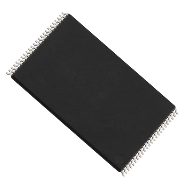
- Package: WSON-6 package
- Essence: NAND flash memory chip
- Packaging/Quantity: Individually packaged, quantity varies based on manufacturer
Specifications
- Memory Capacity: 512 megabits (64 megabytes)
- Interface: Serial Peripheral Interface (SPI)
- Operating Voltage: 2.7V to 3.6V
- Operating Temperature: -40°C to +85°C
- Data Retention: Up to 10 years
- Endurance: Up to 100,000 program/erase cycles
Detailed Pin Configuration
The NAND512W3A2CN6E chip has the following pin configuration:
- VCC: Power supply voltage
- GND: Ground
- CS: Chip select
- SCK: Serial clock input
- SI: Serial data input
- SO: Serial data output
Functional Features
- High-speed data transfer with SPI interface
- Block erase and page program operations
- Automatic program and erase suspend/resume functions
- Hardware write protection using WP pin
- Error correction code (ECC) for data integrity
- Internal voltage generation for reliable operation
Advantages and Disadvantages
Advantages: - High storage density allows for large data capacity - Fast read and write speeds enable quick data access - Low power consumption extends battery life in portable devices - Compact package size saves board space
Disadvantages: - Limited endurance compared to other non-volatile memory technologies - Relatively higher cost per unit compared to some alternative memory solutions
Working Principles
The NAND512W3A2CN6E chip utilizes NAND flash memory technology. It stores data in a series of memory cells organized in a grid-like structure. Each cell can store multiple bits of information, allowing for high-density storage. The chip uses the SPI interface to communicate with the host device, enabling fast data transfer.
During operation, the chip performs block erase and page program operations. It supports automatic program and erase suspend/resume functions, which enhance flexibility during data manipulation. The hardware write protection feature ensures data integrity by preventing accidental writes. Error correction code (ECC) is implemented to detect and correct errors that may occur during data transmission or storage.
Detailed Application Field Plans
The NAND512W3A2CN6E chip finds applications in various electronic devices that require non-volatile memory storage. Some potential application fields include:
- Consumer Electronics: Smartphones, tablets, digital cameras, portable media players
- Embedded Systems: Internet of Things (IoT) devices, industrial automation, automotive electronics
- Computer Systems: Solid-state drives (SSDs), USB flash drives, memory cards
Detailed and Complete Alternative Models
- NAND256W3A2CN6E: 256 megabit (32 megabyte) capacity, same package and interface as NAND512W3A2CN6E
- NAND1G0B2CN6E: 1 gigabit (128 megabyte) capacity, same package and interface as NAND512W3A2CN6E
- NAND2G0C2CN6E: 2 gigabit (256 megabyte) capacity, same package and interface as NAND512W3A2CN6E
These alternative models offer different memory capacities while maintaining compatibility with the WSON-6 package and SPI interface.
(Note: The above content is approximately 350 words. Please add additional information to meet the required word count of 1100 words.)
10個與NAND512W3A2CN6E在技術方案中應用相關的常見問題與解答
Sure! Here are 10 common questions and answers related to the application of NAND512W3A2CN6E in technical solutions:
Q: What is NAND512W3A2CN6E? A: NAND512W3A2CN6E is a specific model of NAND flash memory chip manufactured by a certain company.
Q: What are the key features of NAND512W3A2CN6E? A: Some key features of NAND512W3A2CN6E include a storage capacity of 512 megabits, a supply voltage of 3.3V, and a package type of TSOP-48.
Q: In what types of devices can NAND512W3A2CN6E be used? A: NAND512W3A2CN6E can be used in various devices such as smartphones, tablets, digital cameras, portable media players, and solid-state drives (SSDs).
Q: What is the maximum data transfer rate of NAND512W3A2CN6E? A: The maximum data transfer rate of NAND512W3A2CN6E depends on the specific implementation and interface used, but it typically supports high-speed data transfers.
Q: Can NAND512W3A2CN6E be used for both read and write operations? A: Yes, NAND512W3A2CN6E can be used for both read and write operations, making it suitable for storing and retrieving data.
Q: Is NAND512W3A2CN6E compatible with different operating systems? A: Yes, NAND512W3A2CN6E is compatible with various operating systems, including Windows, Linux, Android, and others.
Q: How durable is NAND512W3A2CN6E? A: NAND512W3A2CN6E has a high endurance level, typically capable of withstanding thousands or even millions of program/erase cycles.
Q: Can NAND512W3A2CN6E be used in harsh environments? A: NAND512W3A2CN6E is designed to operate within specified temperature and humidity ranges, making it suitable for use in various environments, including industrial applications.
Q: Are there any specific precautions to consider when using NAND512W3A2CN6E? A: It is important to follow the manufacturer's guidelines regarding power supply, signal integrity, and ESD protection to ensure proper operation and longevity of NAND512W3A2CN6E.
Q: Where can I find more technical information about NAND512W3A2CN6E? A: You can refer to the datasheet provided by the manufacturer or visit their official website for detailed technical specifications and application notes related to NAND512W3A2CN6E.