

SY100E142JC
Overview
Category: Integrated Circuit (IC)
Use: Digital Logic Device
Characteristics: - High-speed operation - Low power consumption - Wide operating voltage range - Small package size
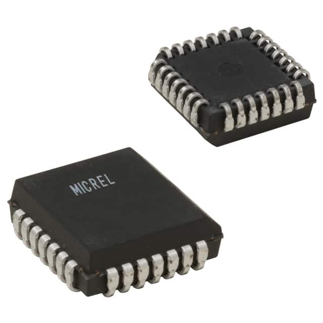
Package: 20-pin PLCC (Plastic Leaded Chip Carrier)
Essence: The SY100E142JC is a digital logic device that operates at high speeds while consuming low power. It is commonly used in applications where fast and efficient data processing is required.
Packaging/Quantity: The SY100E142JC is typically sold in reels or tubes, with each reel/tube containing a specific quantity of ICs. The exact packaging and quantity may vary depending on the supplier.
Specifications
- Supply Voltage Range: 4.2V to 5.7V
- Operating Temperature Range: -40°C to +85°C
- Input Voltage Levels: TTL-compatible
- Output Voltage Levels: ECL-compatible
- Maximum Clock Frequency: 1.6 GHz
- Propagation Delay: 0.8 ns
Pin Configuration
The SY100E142JC has a total of 20 pins, which are labeled as follows:
- CLK
- D0
- D1
- D2
- D3
- D4
- D5
- D6
- D7
- VBB
- Q0
- Q1
- Q2
- Q3
- Q4
- Q5
- Q6
- Q7
- GND
- VCC
Functional Features
- High-speed clocked D-type flip-flop
- Eight data inputs (D0-D7)
- Single clock input (CLK)
- Eight differential outputs (Q0-Q7)
- TTL-compatible input levels
- ECL-compatible output levels
Advantages and Disadvantages
Advantages: - High-speed operation allows for fast data processing - Low power consumption reduces energy usage - Wide operating voltage range provides flexibility in different applications - Small package size saves board space
Disadvantages: - Limited availability of alternative models - Higher cost compared to some other digital logic devices
Working Principles
The SY100E142JC operates based on the principles of clocked D-type flip-flops. It latches the input data (D0-D7) at the rising edge of the clock signal (CLK) and propagates it to the corresponding output pins (Q0-Q7). The device is designed to work with TTL-compatible input levels and provide ECL-compatible output levels.
Application Field Plans
The SY100E142JC finds applications in various fields where high-speed digital data processing is required. Some of the potential application areas include:
- Telecommunications: Used in high-speed data transmission systems, such as optical networks and wireless communication.
- Data Centers: Employed in servers and networking equipment to handle large volumes of data quickly.
- Industrial Automation: Integrated into control systems for real-time monitoring and processing of industrial data.
- Test and Measurement: Utilized in test equipment to analyze and process signals accurately and rapidly.
- Aerospace and Defense: Incorporated into radar systems, avionics, and military communication systems for efficient data handling.
Alternative Models
While the SY100E142JC is a popular choice for high-speed digital logic applications, there are alternative models available from different manufacturers. Some notable alternatives include:
- MC10E141 - ON Semiconductor
- 74FCT16244 - Fairchild Semiconductor
- SN74LVTH16244A - Texas Instruments
- CDCLVD110AVFR - Texas Instruments
These alternative models offer similar functionality and can be considered as substitutes for the SY100E142JC in specific applications.
Note: The above information is subject to change, and it is recommended to refer to the manufacturer's datasheet for the most up-to-date specifications and details.
10個與SY100E142JC在技術方案中應用相關的常見問題與解答
Sure! Here are 10 common questions and answers related to the application of SY100E142JC in technical solutions:
Question: What is SY100E142JC?
Answer: SY100E142JC is a high-speed, low-power ECL (Emitter-Coupled Logic) device used for various digital applications.Question: What is the operating voltage range of SY100E142JC?
Answer: The operating voltage range of SY100E142JC is typically between -4.2V and -5.7V.Question: What is the maximum clock frequency supported by SY100E142JC?
Answer: SY100E142JC can support clock frequencies up to 1.6 GHz.Question: Can SY100E142JC be used in high-speed data communication systems?
Answer: Yes, SY100E142JC is commonly used in high-speed data communication systems, such as fiber optic networks and telecommunications.Question: Does SY100E142JC have built-in input/output termination resistors?
Answer: No, SY100E142JC does not have built-in input/output termination resistors. External termination resistors may be required depending on the application.Question: What is the power consumption of SY100E142JC?
Answer: SY100E142JC has a low power consumption, typically around 400 mW.Question: Can SY100E142JC operate in harsh environments?
Answer: SY100E142JC is designed to operate in industrial temperature ranges (-40°C to +85°C) and can withstand moderate levels of shock and vibration.Question: What are the typical applications of SY100E142JC?
Answer: SY100E142JC is commonly used in applications such as high-speed data transmission, clock distribution, and digital signal processing.Question: Does SY100E142JC support differential signaling?
Answer: Yes, SY100E142JC supports differential signaling, making it suitable for applications that require high noise immunity.Question: Can SY100E142JC be used in battery-powered devices?
Answer: While SY100E142JC is not specifically designed for battery-powered devices due to its higher power consumption, it can still be used with appropriate power management techniques if power efficiency is a concern.
Please note that the answers provided are general and may vary depending on specific application requirements.