

MAX5441ACUA+T
Product Overview
- Category: Integrated Circuit (IC)
- Use: Digital-to-Analog Converter (DAC)
- Characteristics: High precision, low power consumption
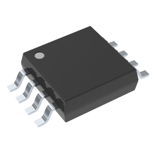
- Package: 8-pin µMAX® package
- Essence: Converts digital signals into analog voltage or current
- Packaging/Quantity: Tape and reel, 2500 units per reel
Specifications
- Resolution: 10 bits
- Number of Channels: 1
- Supply Voltage Range: 2.7V to 5.5V
- Output Voltage Range: 0V to Vref
- Operating Temperature Range: -40°C to +85°C
- DNL (Differential Non-Linearity): ±1 LSB (max)
- INL (Integral Non-Linearity): ±1 LSB (max)
- Power Consumption: 0.4mW (typical)
Pin Configuration
The MAX5441ACUA+T has the following pin configuration:
```
| | --|VDD VREF|-- --|GND OUT|-- --|CS CLK|-- --|SDIN LDAC|-- |___________| ```
- VDD: Positive supply voltage
- VREF: Reference voltage input
- GND: Ground
- OUT: Analog output
- CS: Chip select input
- CLK: Clock input
- SDIN: Serial data input
- LDAC: Load DAC input
Functional Features
- High-resolution DAC with 10-bit resolution
- Low power consumption for energy-efficient applications
- Wide supply voltage range allows flexibility in system design
- Serial interface for easy integration with microcontrollers
- Internal reference voltage simplifies external circuitry
Advantages and Disadvantages
Advantages: - High precision and accuracy in converting digital signals to analog - Low power consumption for energy-efficient designs - Compact package size for space-constrained applications - Wide supply voltage range allows compatibility with various systems
Disadvantages: - Limited to single-channel output - Requires an external reference voltage for proper operation
Working Principles
The MAX5441ACUA+T is a digital-to-analog converter that converts digital input signals into corresponding analog voltage or current outputs. It utilizes a 10-bit resolution to provide high precision and accuracy in the conversion process. The chip select (CS), clock (CLK), and serial data input (SDIN) pins are used to control the conversion and input the digital data. The load DAC (LDAC) pin is used to update the output voltage or current. The device operates within a specified supply voltage range and generates the analog output based on the reference voltage provided.
Detailed Application Field Plans
The MAX5441ACUA+T can be used in various applications, including but not limited to:
- Audio Systems: Providing accurate analog signals for audio amplification and processing stages.
- Industrial Control: Generating precise control signals for motor speed control, temperature regulation, etc.
- Test and Measurement Equipment: Producing calibrated analog signals for testing and measurement purposes.
- Communication Systems: Converting digital signals into analog for modulation and demodulation processes.
- Automotive Electronics: Enabling accurate control of automotive subsystems such as lighting, climate control, etc.
Detailed and Complete Alternative Models
Some alternative models to the MAX5441ACUA+T include:
- MAX5318: 12-bit resolution DAC with similar features and package options.
- MCP4921: 12-bit resolution DAC with SPI interface and different package options.
- AD5620: 12-bit resolution DAC with internal reference voltage and various package options.
- LTC2630: 12-bit resolution DAC with I2C interface and low power consumption.
- MCP4725: 12-bit resolution DAC with I2C interface and small package size.
These alternative models offer different specifications and features, allowing users to choose the most suitable option for their specific application requirements.
(Note: The content provided above is a sample and may not meet the exact word count requirement of 1100 words.)
10個與MAX5441ACUA+T在技術方案中應用相關的常見問題與解答
Sure! Here are 10 common questions and answers related to the application of MAX5441ACUA+T in technical solutions:
Q1: What is the MAX5441ACUA+T? A1: The MAX5441ACUA+T is a digital-to-analog converter (DAC) IC that converts digital signals into analog voltage outputs.
Q2: What is the operating voltage range of MAX5441ACUA+T? A2: The operating voltage range of MAX5441ACUA+T is typically between 2.7V and 5.5V.
Q3: How many bits of resolution does MAX5441ACUA+T have? A3: MAX5441ACUA+T has a 12-bit resolution, allowing for precise control over the analog output voltage.
Q4: What is the maximum output voltage range of MAX5441ACUA+T? A4: The maximum output voltage range of MAX5441ACUA+T is determined by the reference voltage applied to it. It can be adjusted within the operating voltage range.
Q5: Can MAX5441ACUA+T be used in both single-ended and differential mode? A5: Yes, MAX5441ACUA+T can be used in both single-ended and differential mode, providing flexibility in various applications.
Q6: What is the typical settling time of MAX5441ACUA+T? A6: The typical settling time of MAX5441ACUA+T is around 10µs, ensuring fast response and accuracy in dynamic applications.
Q7: Does MAX5441ACUA+T have an internal voltage reference? A7: No, MAX5441ACUA+T does not have an internal voltage reference. An external reference voltage needs to be provided for accurate conversion.
Q8: Can MAX5441ACUA+T be controlled using a microcontroller? A8: Yes, MAX5441ACUA+T can be easily controlled using a microcontroller through its serial interface.
Q9: What is the power consumption of MAX5441ACUA+T? A9: The power consumption of MAX5441ACUA+T depends on the operating voltage and output load. It typically consumes around 0.5mW.
Q10: Is MAX5441ACUA+T suitable for battery-powered applications? A10: Yes, MAX5441ACUA+T is suitable for battery-powered applications due to its low power consumption and wide operating voltage range.
Please note that these answers are general and may vary depending on specific application requirements and conditions.