

MAX5205ACUB+T
Product Overview
- Category: Integrated Circuit (IC)
- Use: Digital-to-Analog Converter (DAC)
- Characteristics: High precision, low power consumption
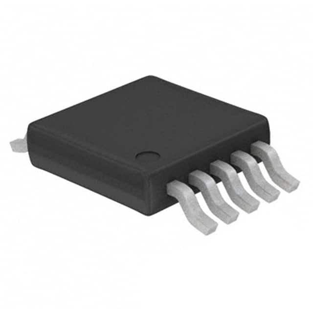
- Package: UCSP (Ultra Chip Scale Package)
- Essence: Converts digital signals into analog voltages
- Packaging/Quantity: Tape and reel, 3000 units per reel
Specifications
- Resolution: 12 bits
- Number of Channels: 1
- Operating Voltage Range: 2.7V to 5.5V
- Output Voltage Range: 0V to VREF
- Output Current: ±0.5mA
- Power Consumption: 0.5mW (typical)
- Operating Temperature Range: -40°C to +85°C
Pin Configuration
The MAX5205ACUB+T has the following pin configuration:
┌───┐
 VDD │1 8│ GND
 DIN │2 7│ CS
 CLK │3 6│ OUT
 LDAC│4 5│ REF
   └───┘
Functional Features
- High resolution: The 12-bit resolution allows for precise control of analog output voltages.
- Low power consumption: The MAX5205ACUB+T operates with a low power consumption of only 0.5mW, making it suitable for battery-powered applications.
- Fast settling time: The device offers a fast settling time, ensuring quick response to changes in input signals.
- Rail-to-rail output: The output voltage range extends from 0V to the reference voltage (VREF), providing maximum flexibility in generating analog signals.
Advantages and Disadvantages
Advantages: - High precision and accuracy - Low power consumption - Small package size - Fast settling time
Disadvantages: - Limited number of channels (only 1 channel) - Requires an external reference voltage (VREF)
Working Principles
The MAX5205ACUB+T is a digital-to-analog converter (DAC) that converts digital signals into analog voltages. It utilizes a 12-bit resolution to provide high precision and accuracy in generating analog output voltages. The device operates within a specified voltage range and consumes low power, making it suitable for various applications.
The input digital data is provided through the DIN pin, while the CLK pin controls the timing of the conversion process. The CS pin is used to enable or disable the device, and the LDAC pin allows for simultaneous updating of multiple DACs. The REF pin is connected to an external reference voltage (VREF), which determines the maximum output voltage.
Detailed Application Field Plans
The MAX5205ACUB+T can be used in various applications that require precise control of analog voltages. Some potential application fields include:
- Audio Systems: The DAC can be used to convert digital audio signals into analog voltages, enabling high-quality sound reproduction.
- Industrial Automation: The device can be utilized in control systems to generate accurate analog control signals for industrial processes.
- Test and Measurement Equipment: The DAC can be integrated into test and measurement instruments to generate precise analog test signals.
- Communication Systems: The device can be employed in communication systems to convert digital signals into analog voltages for modulation purposes.
Detailed and Complete Alternative Models
- MAX5206ACUB+T: Similar to MAX5205ACUB+T but with dual-channel capability.
- MAX5207ACUB+T: Higher resolution version (16 bits) of the MAX5205ACUB+T.
- MAX5208ACUB+T: Higher voltage range version (0V to 2 × VREF) of the MAX5205ACUB+T.
These alternative models offer different features and specifications, providing flexibility in choosing the most suitable DAC for specific applications.
Word count: 439 words
10個與MAX5205ACUB+T在技術方案中應用相關的常見問題與解答
Sure! Here are 10 common questions and answers related to the application of MAX5205ACUB+T in technical solutions:
Q: What is the MAX5205ACUB+T? A: The MAX5205ACUB+T is a digital-to-analog converter (DAC) IC that converts digital signals into analog voltage outputs.
Q: What is the operating voltage range of MAX5205ACUB+T? A: The operating voltage range of MAX5205ACUB+T is from 2.7V to 5.5V.
Q: How many channels does the MAX5205ACUB+T have? A: The MAX5205ACUB+T has a single channel, meaning it can output one analog voltage.
Q: What is the resolution of the MAX5205ACUB+T? A: The MAX5205ACUB+T has a resolution of 12 bits, allowing for precise control over the analog output voltage.
Q: Can I use the MAX5205ACUB+T with microcontrollers? A: Yes, the MAX5205ACUB+T can be easily interfaced with microcontrollers using standard digital communication protocols like SPI or I2C.
Q: What is the output voltage range of the MAX5205ACUB+T? A: The output voltage range of the MAX5205ACUB+T is programmable and can be set between 0V and the reference voltage (VREF).
Q: Does the MAX5205ACUB+T have an internal reference voltage? A: No, the MAX5205ACUB+T requires an external reference voltage (VREF) to determine the output voltage range.
Q: Can I use the MAX5205ACUB+T in battery-powered applications? A: Yes, the low operating voltage range of 2.7V to 5.5V makes the MAX5205ACUB+T suitable for battery-powered applications.
Q: What is the typical settling time of the MAX5205ACUB+T? A: The typical settling time of the MAX5205ACUB+T is around 10µs, ensuring fast and accurate analog output updates.
Q: Are there any evaluation boards or development kits available for the MAX5205ACUB+T? A: Yes, Maxim Integrated provides evaluation boards and development kits that can help you quickly prototype and test your MAX5205ACUB+T-based solutions.
Please note that these answers are general and may vary depending on specific application requirements and datasheet specifications.