

DG409CY+T
Product Overview
- Category: Integrated Circuit (IC)
- Use: Analog Multiplexer/Demultiplexer
- Characteristics: High-speed, low-power consumption, wide voltage range
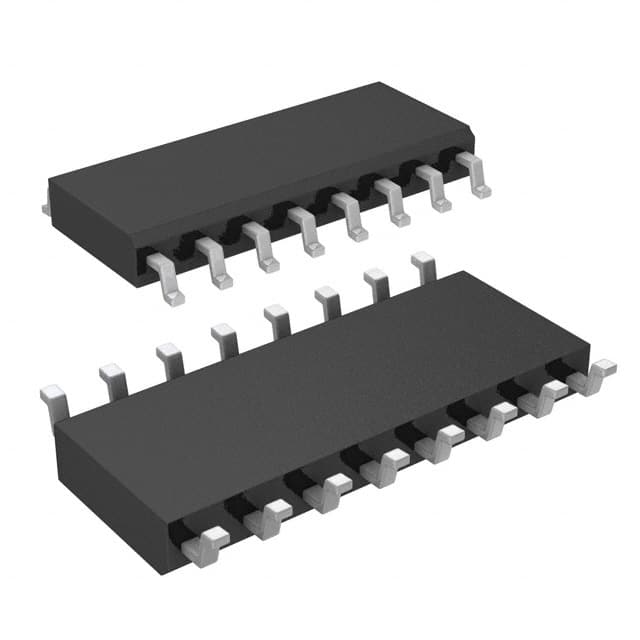
- Package: 16-pin SOIC (Small Outline Integrated Circuit)
- Essence: A versatile IC used for signal routing and switching in various electronic applications
- Packaging/Quantity: Available in reels of 2500 units
Specifications
- Supply Voltage Range: ±2V to ±18V
- On-Resistance: 80Ω (typical)
- Channel-to-Channel Matching: 5Ω (typical)
- Operating Temperature Range: -40°C to +85°C
- Input Signal Range: ±15V
- Bandwidth: 100MHz (typical)
Detailed Pin Configuration
- IN1: Input control pin for channel 1
- IN2: Input control pin for channel 2
- IN3: Input control pin for channel 3
- IN4: Input control pin for channel 4
- VEE: Negative power supply
- GND: Ground
- OUT: Output pin
- INH: Inhibit control pin
- NC: No connection
- VCC: Positive power supply
- IN5: Input control pin for channel 5
- IN6: Input control pin for channel 6
- IN7: Input control pin for channel 7
- IN8: Input control pin for channel 8
- S1: Channel select input 1
- S0: Channel select input 0
Functional Features
- Signal Routing: The DG409CY+T allows the selection of one out of eight input channels to be routed to the output pin.
- Low Power Consumption: The IC operates with low power consumption, making it suitable for battery-powered devices.
- High-Speed Operation: With a bandwidth of 100MHz, the DG409CY+T can handle high-frequency signals efficiently.
- Wide Voltage Range: The IC supports a wide supply voltage range, enabling compatibility with various electronic systems.
Advantages and Disadvantages
Advantages
- Versatile multiplexer/demultiplexer solution
- Low power consumption
- High-speed operation
- Wide voltage range support
Disadvantages
- Limited number of channels (8)
- Relatively high on-resistance
Working Principles
The DG409CY+T is based on CMOS technology and utilizes analog switches to route signals. It operates by selectively connecting one of the eight input channels to the output pin based on the control inputs. The IC's internal circuitry ensures minimal signal distortion and low power consumption during operation.
Detailed Application Field Plans
The DG409CY+T finds applications in various fields, including:
- Audio Systems: Used for audio signal routing in mixers, amplifiers, and audio interfaces.
- Test and Measurement Equipment: Enables channel switching in data acquisition systems and test instruments.
- Communication Systems: Facilitates signal routing in telecommunication devices and network switches.
- Industrial Automation: Utilized for signal selection in control systems and industrial machinery.
- Medical Devices: Enables signal routing in medical imaging equipment and patient monitoring systems.
Detailed and Complete Alternative Models
- CD74HC4067: 16-channel analog multiplexer/demultiplexer with similar characteristics.
- ADG408: 8-channel analog multiplexer/demultiplexer with lower on-resistance.
- MAX4617: 8-channel analog switch with higher bandwidth.
(Note: This list is not exhaustive and serves as a reference for alternative models.)
Word count: 408 words
10個與DG409CY+T在技術方案中應用相關的常見問題與解答
Sure! Here are 10 common questions and answers related to the application of DG409CY+T in technical solutions:
Q: What is DG409CY+T? A: DG409CY+T is a multiplexer/demultiplexer integrated circuit (IC) that allows multiple signals to be routed through a single channel.
Q: What are the key features of DG409CY+T? A: Some key features of DG409CY+T include low on-resistance, wide voltage range, low power consumption, and compatibility with various logic levels.
Q: How can DG409CY+T be used in technical solutions? A: DG409CY+T can be used in applications such as signal routing, analog switching, audio/video signal processing, data acquisition systems, and test equipment.
Q: What is the voltage range supported by DG409CY+T? A: DG409CY+T supports a wide voltage range, typically from -5V to +20V, making it suitable for both analog and digital signals.
Q: Can DG409CY+T handle high-frequency signals? A: Yes, DG409CY+T has a high bandwidth and can handle high-frequency signals up to several megahertz.
Q: Is DG409CY+T compatible with different logic levels? A: Yes, DG409CY+T is compatible with various logic levels, including TTL, CMOS, and LVCMOS.
Q: What is the on-resistance of DG409CY+T? A: The on-resistance of DG409CY+T is typically very low, usually in the range of a few ohms.
Q: Can DG409CY+T be used in battery-powered devices? A: Yes, DG409CY+T has low power consumption, making it suitable for battery-powered devices and portable applications.
Q: Are there any specific precautions to consider when using DG409CY+T? A: It is important to ensure that the voltage levels and signal characteristics are within the specified limits of DG409CY+T to avoid any damage or performance issues.
Q: Where can I find more information about DG409CY+T and its application notes? A: You can refer to the datasheet and application notes provided by the manufacturer of DG409CY+T for detailed information on its usage and recommended circuit configurations.
Please note that the answers provided here are general and may vary depending on the specific requirements and use cases.