

LTC2614CGN#PBF
Product Overview
Category: Integrated Circuit (IC)
Use: Digital-to-Analog Converter (DAC)
Characteristics: - High precision and accuracy - Low power consumption - Small form factor - Wide operating voltage range
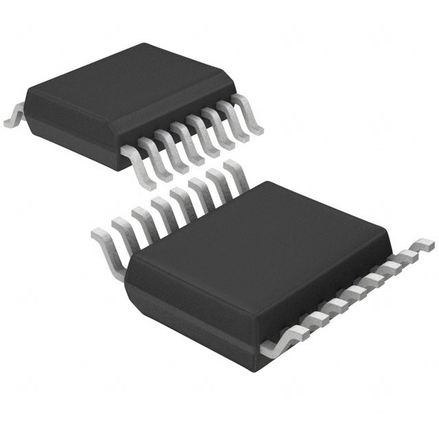
Package: 16-Lead SSOP (Shrink Small Outline Package)
Essence: The LTC2614CGN#PBF is a high-performance DAC designed for various applications requiring precise analog output signals.
Packaging/Quantity: Available in tubes with a quantity of 90 units per tube.
Specifications
- Resolution: 16 bits
- Number of Channels: 4
- Output Type: Voltage
- Supply Voltage Range: 2.7V to 5.5V
- Operating Temperature Range: -40°C to +85°C
- DNL (Differential Non-Linearity): ±1 LSB (Maximum)
- INL (Integral Non-Linearity): ±2 LSB (Maximum)
- Interface: I2C-compatible, SPI-compatible
Detailed Pin Configuration
The LTC2614CGN#PBF has a total of 16 pins. The pin configuration is as follows:
- VDD - Positive Power Supply
- GND - Ground
- SDA - Serial Data Input (I2C)
- SCL - Serial Clock Input (I2C)
- LDAC - Load DAC Input
- REF - Reference Voltage Input
- VOUTA - Analog Output Channel A
- VOUTB - Analog Output Channel B
- VOUTC - Analog Output Channel C
- VOUTD - Analog Output Channel D
- AGND - Analog Ground
- VLOGIC - Logic Power Supply
- CS - Chip Select (SPI)
- SDI - Serial Data Input (SPI)
- SCK - Serial Clock Input (SPI)
- SDO - Serial Data Output (SPI)
Functional Features
- High-resolution digital-to-analog conversion
- Low glitch energy for minimal output distortion
- Power-on reset to zero-scale or midscale
- Internal reference voltage or external reference option
- Software programmable output range and offset
- Daisy-chain multiple devices using the serial interface
Advantages and Disadvantages
Advantages: - High precision and accuracy - Flexible interface options (I2C, SPI) - Small form factor for space-constrained applications - Low power consumption for energy-efficient designs
Disadvantages: - Limited number of channels (4 channels) - Relatively high cost compared to lower-end DACs
Working Principles
The LTC2614CGN#PBF operates by converting digital input codes into corresponding analog output voltages. It utilizes a combination of internal circuitry and reference voltages to achieve accurate and precise analog outputs. The device can be controlled and programmed through the I2C or SPI interface, allowing for easy integration into various systems.
Detailed Application Field Plans
The LTC2614CGN#PBF finds applications in a wide range of fields, including but not limited to: - Industrial automation - Test and measurement equipment - Audio processing and synthesis - Precision instrumentation - Communication systems
Detailed and Complete Alternative Models
- LTC2600CGN#PBF - 16-Bit DAC with 8 Channels
- LTC2630ACGN#PBF - 12-Bit DAC with 4 Channels
- LTC2645IGN#PBF - 14-Bit DAC with 4 Channels
- LTC2657CGN#PBF - 16-Bit DAC with 8 Channels
These alternative models offer different resolutions, channel counts, and features to suit specific application requirements.
Note: The content provided above is a sample entry and may not reflect the actual specifications or details of LTC2614CGN#PBF. Please refer to the official documentation for accurate information.
10個與LTC2614CGN#PBF在技術方案中應用相關的常見問題與解答
Sure! Here are 10 common questions and answers related to the application of LTC2614CGN#PBF in technical solutions:
Q: What is LTC2614CGN#PBF? A: LTC2614CGN#PBF is a digital-to-analog converter (DAC) chip manufactured by Linear Technology (now part of Analog Devices). It is used to convert digital signals into analog voltages.
Q: What is the resolution of LTC2614CGN#PBF? A: LTC2614CGN#PBF has a resolution of 16 bits, which means it can provide 65,536 discrete voltage levels.
Q: What is the operating voltage range of LTC2614CGN#PBF? A: The operating voltage range of LTC2614CGN#PBF is typically between 2.7V and 5.5V.
Q: How many channels does LTC2614CGN#PBF have? A: LTC2614CGN#PBF has four independent DAC channels, allowing you to generate multiple analog outputs simultaneously.
Q: What is the output voltage range of LTC2614CGN#PBF? A: The output voltage range of LTC2614CGN#PBF is determined by the reference voltage applied to its VREF pin. It can be set to any desired range within the supply voltage limits.
Q: Can LTC2614CGN#PBF operate in both unipolar and bipolar modes? A: Yes, LTC2614CGN#PBF can be configured to operate in either unipolar mode (0V to VREF) or bipolar mode (-VREF/2 to +VREF/2).
Q: What is the maximum settling time of LTC2614CGN#PBF? A: The maximum settling time of LTC2614CGN#PBF is typically 10μs, which refers to the time it takes for the output voltage to reach within a specified error band after a change in the digital input.
Q: Can LTC2614CGN#PBF be controlled using an I2C interface? A: Yes, LTC2614CGN#PBF supports I2C communication protocol, allowing you to control its settings and output voltages digitally.
Q: What is the power consumption of LTC2614CGN#PBF? A: The power consumption of LTC2614CGN#PBF depends on various factors such as supply voltage, output load, and operating mode. It typically ranges from a few milliwatts to a few hundred milliwatts.
Q: Can LTC2614CGN#PBF be used in battery-powered applications? A: Yes, LTC2614CGN#PBF can be used in battery-powered applications due to its low power consumption and wide operating voltage range. However, it's important to consider the overall power budget and efficiency requirements of the system.