

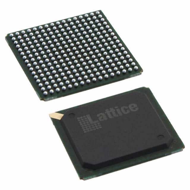
LFXP6C-3F256C
Product Overview
Category
The LFXP6C-3F256C belongs to the category of Field Programmable Gate Arrays (FPGAs).
Use
FPGAs are integrated circuits that can be programmed and reprogrammed to perform various digital functions. The LFXP6C-3F256C is specifically designed for applications requiring high-performance and low-power consumption.
Characteristics
- High-performance FPGA with low power consumption
- Flexible and reprogrammable design
- Suitable for a wide range of applications
- Compact package size
Package
The LFXP6C-3F256C is available in a compact package, ensuring easy integration into electronic systems.
Essence
The essence of the LFXP6C-3F256C lies in its ability to provide high-performance digital functionality while consuming minimal power.
Packaging/Quantity
The LFXP6C-3F256C is typically packaged individually and is available in various quantities depending on the requirements of the user.
Specifications
- FPGA Family: LatticeXP2
- Logic Cells: 6,080
- Flip-Flops: 12,160
- Block RAM: 288 Kbits
- Maximum User I/Os: 266
- Operating Voltage: 1.2V
- Speed Grade: -3
- Package Type: FBGA
- Package Pins: 256
Detailed Pin Configuration
For a detailed pin configuration of the LFXP6C-3F256C, please refer to the manufacturer's datasheet or technical documentation.
Functional Features
- High-performance digital processing capabilities
- Low power consumption for energy-efficient operation
- Reprogrammable design allows for flexibility in implementing different functionalities
- Support for various communication protocols and interfaces
- On-chip memory resources for efficient data storage and processing
Advantages and Disadvantages
Advantages
- High-performance capabilities suitable for demanding applications
- Low power consumption for energy-efficient operation
- Flexible and reprogrammable design allows for customization
- Compact package size enables easy integration into electronic systems
Disadvantages
- Limited availability of alternative models with similar specifications
- Steep learning curve for programming and utilizing the FPGA's full potential
Working Principles
The LFXP6C-3F256C operates based on the principles of digital logic. It consists of configurable logic blocks, interconnects, and input/output elements. The user can program the FPGA to implement specific digital functions by configuring the logic blocks and interconnects using a hardware description language (HDL) or a graphical design tool.
Detailed Application Field Plans
The LFXP6C-3F256C finds applications in various fields, including but not limited to: - Telecommunications - Industrial automation - Automotive electronics - Aerospace and defense - Medical devices - Consumer electronics
In telecommunications, the FPGA can be used for signal processing, protocol conversion, and network optimization. In industrial automation, it can enable real-time control and monitoring of manufacturing processes. In automotive electronics, it can support advanced driver assistance systems (ADAS) and infotainment functionalities. In aerospace and defense, it can be utilized for radar and communication systems. In medical devices, it can assist in image processing and diagnostics. In consumer electronics, it can enhance the performance and functionality of devices such as smartphones and gaming consoles.
Detailed and Complete Alternative Models
While the LFXP6C-3F256C offers unique features and specifications, there are alternative models available from different manufacturers that provide similar functionality. Some notable alternatives include: - Xilinx Virtex-7 series - Intel (formerly Altera) Cyclone V series - Microsemi (formerly Actel) SmartFusion2 series
These alternative models offer a range of options in terms of logic capacity, I/O count, power consumption, and package size. Users should carefully evaluate their specific requirements and select the most suitable FPGA for their application.
Note: The content provided above is an overview and may not cover all aspects of the LFXP6C-3F256C. For detailed technical information, please refer to the manufacturer's documentation.
10個與LFXP6C-3F256C在技術方案中應用相關的常見問題與解答
Sure! Here are 10 common questions and answers related to the application of LFXP6C-3F256C in technical solutions:
Q: What is the LFXP6C-3F256C? A: The LFXP6C-3F256C is a field-programmable gate array (FPGA) manufactured by Lattice Semiconductor.
Q: What are the key features of the LFXP6C-3F256C? A: The key features include 6,080 Look-Up Tables (LUTs), 256 I/O pins, 256 kilobits of embedded memory, and support for various communication protocols.
Q: What are some typical applications of the LFXP6C-3F256C? A: The LFXP6C-3F256C is commonly used in applications such as industrial automation, telecommunications, automotive systems, medical devices, and consumer electronics.
Q: How can I program the LFXP6C-3F256C? A: The LFXP6C-3F256C can be programmed using hardware description languages (HDLs) like VHDL or Verilog, along with design software provided by Lattice Semiconductor.
Q: Can the LFXP6C-3F256C be reprogrammed after deployment? A: Yes, the LFXP6C-3F256C is a reprogrammable FPGA, allowing for flexibility and updates to the design even after deployment.
Q: What are the power requirements for the LFXP6C-3F256C? A: The LFXP6C-3F256C typically operates at a voltage range of 1.14V to 1.26V, with power consumption varying based on the design and usage.
Q: Does the LFXP6C-3F256C support high-speed interfaces? A: Yes, the LFXP6C-3F256C supports various high-speed interfaces such as LVDS, DDR3, PCIe, and Ethernet, making it suitable for applications requiring fast data transfer.
Q: Can I use the LFXP6C-3F256C in a mixed-signal design? A: While the LFXP6C-3F256C is primarily a digital device, it can be used in conjunction with analog components to create mixed-signal designs.
Q: Are there any development boards available for the LFXP6C-3F256C? A: Yes, Lattice Semiconductor provides development boards like the LFXP6C-3F256C-EVN, which allow for easy prototyping and evaluation of the FPGA.
Q: Where can I find technical documentation and support for the LFXP6C-3F256C? A: Technical documentation, datasheets, reference designs, and support resources for the LFXP6C-3F256C can be found on the official website of Lattice Semiconductor.