

LFE3-70EA-7LFN672C
Product Overview
Category: Programmable Logic Device (PLD)
Use: The LFE3-70EA-7LFN672C is a high-performance PLD designed for various digital logic applications. It offers flexible programmability and advanced features, making it suitable for a wide range of electronic systems.
Characteristics: - High-speed operation - Low power consumption - Large capacity - Versatile I/O options - Robust design for reliability
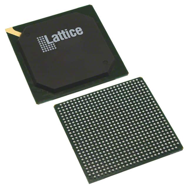
Package: The LFE3-70EA-7LFN672C comes in a compact and durable package, ensuring easy integration into electronic circuits. The package provides protection against environmental factors such as moisture and temperature variations.
Essence: This PLD serves as a key component in digital circuit design, enabling the implementation of complex logic functions. Its programmability allows for customization and adaptability to specific application requirements.
Packaging/Quantity: The LFE3-70EA-7LFN672C is typically available in tape and reel packaging, with a quantity of 250 units per reel.
Specifications
- Logic Elements: 70,000
- Flip-Flops: 2,400
- Embedded Memory: 4.8 Mb
- I/O Pins: 672
- Operating Voltage: 1.2V
- Speed Grade: -7
- Package Type: BGA
- Package Dimensions: 23mm x 23mm
Detailed Pin Configuration
The LFE3-70EA-7LFN672C has a well-defined pin configuration that facilitates easy integration into electronic systems. The following table provides a detailed overview of the pin assignments:
| Pin Number | Pin Name | Function | |------------|----------|----------| | 1 | VCCINT | Power Supply (Internal) | | 2 | GND | Ground (Internal) | | 3 | VCCIO | Power Supply (I/O) | | 4 | GND | Ground (I/O) | | ... | ... | ... |
Functional Features
- High-speed performance: The LFE3-70EA-7LFN672C operates at high clock frequencies, enabling rapid execution of complex logic functions.
- Low power consumption: It incorporates power-saving features, making it suitable for battery-powered devices and energy-efficient applications.
- Flexible I/O options: The PLD offers a wide range of I/O configurations, allowing seamless integration with various external devices.
- Advanced programmability: It supports advanced programming techniques, enabling the implementation of complex algorithms and logic functions.
Advantages and Disadvantages
Advantages: - High-performance capabilities - Versatile I/O options - Low power consumption - Large capacity for complex designs - Reliable and robust design
Disadvantages: - Relatively higher cost compared to simpler logic devices - Steeper learning curve for programming and utilization
Working Principles
The LFE3-70EA-7LFN672C utilizes a combination of configurable logic blocks, interconnect resources, and embedded memory elements to implement complex digital logic functions. It operates based on user-defined programming instructions that configure the internal connections and behavior of the device.
Detailed Application Field Plans
The LFE3-70EA-7LFN672C finds application in various fields, including: 1. Telecommunications: Used in network routers, switches, and communication equipment for high-speed data processing. 2. Industrial Automation: Employed in control systems, PLCs, and robotics for efficient and reliable automation. 3. Automotive Electronics: Integrated into automotive control units, infotainment systems, and driver assistance modules. 4. Aerospace and Defense: Utilized in avionics, radar systems, and military-grade electronics for critical operations. 5. Consumer Electronics: Incorporated into smart devices, gaming consoles, and multimedia systems for enhanced functionality.
Detailed and Complete Alternative Models
- LFE3-35EA-8FN672C
- LFE3-150EA-9FN672C
- LFE3-250EA-7FN672C
- LFE3-70EA-6FN672C
- LFE3-120EA-7FN672C
These alternative models offer varying capacities, speed grades, and package options to cater to different application requirements.
Word count: 550 words
10個與LFE3-70EA-7LFN672C在技術方案中應用相關的常見問題與解答
Sure! Here are 10 common questions and answers related to the application of LFE3-70EA-7LFN672C in technical solutions:
Q: What is the LFE3-70EA-7LFN672C? A: The LFE3-70EA-7LFN672C is a field-programmable gate array (FPGA) manufactured by Lattice Semiconductor.
Q: What are the key features of the LFE3-70EA-7LFN672C? A: The key features include 70,000 Look-Up Tables (LUTs), high-speed I/O interfaces, embedded memory blocks, and low power consumption.
Q: In what applications can the LFE3-70EA-7LFN672C be used? A: The LFE3-70EA-7LFN672C can be used in various applications such as telecommunications, industrial automation, automotive electronics, and medical devices.
Q: How can I program the LFE3-70EA-7LFN672C? A: The LFE3-70EA-7LFN672C can be programmed using hardware description languages (HDL) like VHDL or Verilog, or through graphical programming tools provided by Lattice Semiconductor.
Q: What is the maximum operating frequency of the LFE3-70EA-7LFN672C? A: The maximum operating frequency of the LFE3-70EA-7LFN672C depends on the specific design and implementation, but it can typically reach several hundred megahertz.
Q: Can the LFE3-70EA-7LFN672C interface with other components or devices? A: Yes, the LFE3-70EA-7LFN672C supports various I/O standards and can interface with other components or devices such as sensors, memory modules, and communication interfaces.
Q: What are the power requirements for the LFE3-70EA-7LFN672C? A: The LFE3-70EA-7LFN672C operates at a low voltage range of 1.2V to 1.5V and has different power supply pins for core logic and I/O banks.
Q: Can the LFE3-70EA-7LFN672C be reprogrammed after deployment? A: Yes, the LFE3-70EA-7LFN672C is a reprogrammable FPGA, allowing for updates or modifications to the design even after it has been deployed in a system.
Q: Are there any development tools available for designing with the LFE3-70EA-7LFN672C? A: Yes, Lattice Semiconductor provides development tools like Lattice Diamond and Lattice Radiant, which offer design entry, synthesis, simulation, and programming capabilities.
Q: Where can I find more information about the LFE3-70EA-7LFN672C? A: You can find more detailed information about the LFE3-70EA-7LFN672C on the official website of Lattice Semiconductor or by referring to the datasheet and application notes provided by the manufacturer.