

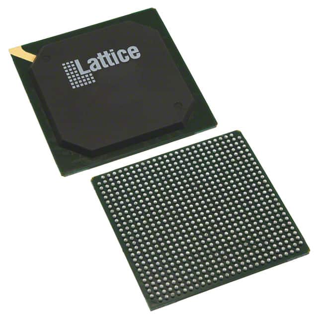
LFE3-35EA-6FN672C
Product Overview
Category
The LFE3-35EA-6FN672C belongs to the category of Field Programmable Gate Arrays (FPGAs).
Use
This FPGA is commonly used in various electronic devices and systems for digital logic implementation, such as communication equipment, industrial control systems, and consumer electronics.
Characteristics
- High-performance programmable logic device
- Offers flexibility and reconfigurability
- Provides a wide range of logic gates, memory blocks, and input/output pins
- Capable of implementing complex digital circuits
- Supports high-speed data processing and signal routing
Package
The LFE3-35EA-6FN672C comes in a compact and durable package, ensuring protection during handling and installation.
Essence
The essence of the LFE3-35EA-6FN672C lies in its ability to provide a customizable and versatile solution for digital circuit design and implementation.
Packaging/Quantity
Each LFE3-35EA-6FN672C unit is packaged individually and is typically sold in quantities suitable for both small-scale and large-scale production.
Specifications
- FPGA Family: LatticeECP3
- Logic Elements: 35,000
- Number of I/O Pins: 672
- Operating Voltage: 1.2V
- Maximum Frequency: 500 MHz
- Embedded Memory: Up to 4.8 Mb
- Configuration Memory: On-chip Flash
Detailed Pin Configuration
The LFE3-35EA-6FN672C has a total of 672 pins, which are divided into different categories based on their functionality. The pin configuration includes:
- Power supply pins
- Ground pins
- Input pins
- Output pins
- Clock pins
- Configuration pins
- Special function pins
For a detailed pin configuration diagram, please refer to the manufacturer's datasheet.
Functional Features
- High-speed data processing capabilities
- Flexible and reconfigurable architecture
- Support for various communication protocols
- On-chip memory blocks for efficient data storage
- Low power consumption
- Built-in security features for protecting intellectual property
Advantages
- Versatile and customizable solution for digital circuit design
- Faster time-to-market due to reprogrammability
- Lower development costs compared to custom ASICs
- Ability to adapt to changing requirements through reconfiguration
- High-performance computing capabilities
Disadvantages
- Higher power consumption compared to dedicated hardware solutions
- Limited resources for complex designs
- Steeper learning curve for inexperienced users
- Higher cost per unit compared to traditional logic gates
Working Principles
The LFE3-35EA-6FN672C operates based on the principles of configurable logic. It consists of a matrix of programmable logic elements interconnected by configurable routing channels. The device can be programmed using Hardware Description Languages (HDL) or graphical tools to define the desired functionality of the digital circuit.
Detailed Application Field Plans
The LFE3-35EA-6FN672C finds applications in various fields, including:
- Communication Equipment: Used for implementing high-speed data processing, protocol conversion, and signal routing in routers, switches, and network infrastructure.
- Industrial Control Systems: Enables the implementation of complex control algorithms, sensor interfacing, and real-time monitoring in industrial automation systems.
- Consumer Electronics: Utilized in devices such as smart TVs, gaming consoles, and home automation systems for advanced functionality and connectivity.
Detailed and Complete Alternative Models
- Xilinx Virtex UltraScale+ FPGA
- Intel Stratix 10 FPGA
- Microsemi PolarFire FPGA
- QuickLogic EOS S3 FPGA
- Actel Fusion FPGA
These alternative models offer similar capabilities and can be considered as alternatives to the LFE3-35EA-6FN672C based on specific project requirements.
Note: The content provided above is an example and may not reflect actual specifications or information about the LFE3-35EA-6FN672C. Please refer to the manufacturer's documentation for accurate details.
10個與LFE3-35EA-6FN672C在技術方案中應用相關的常見問題與解答
Sure! Here are 10 common questions and answers related to the application of LFE3-35EA-6FN672C in technical solutions:
Q: What is the LFE3-35EA-6FN672C? A: The LFE3-35EA-6FN672C is a specific model of FPGA (Field-Programmable Gate Array) manufactured by Lattice Semiconductor.
Q: What are the key features of the LFE3-35EA-6FN672C? A: Some key features of this FPGA include 35,000 Look-Up Tables (LUTs), 672-pin FineLine BGA package, low power consumption, and high-speed performance.
Q: In what applications can the LFE3-35EA-6FN672C be used? A: This FPGA can be used in various applications such as industrial automation, telecommunications, automotive electronics, medical devices, and aerospace systems.
Q: How can I program the LFE3-35EA-6FN672C? A: The LFE3-35EA-6FN672C can be programmed using Lattice Diamond design software or other compatible programming tools provided by Lattice Semiconductor.
Q: What is the power supply requirement for the LFE3-35EA-6FN672C? A: The recommended power supply voltage for this FPGA is typically 1.2V, but it can operate within a range of 1.14V to 1.26V.
Q: Can I interface the LFE3-35EA-6FN672C with external devices? A: Yes, this FPGA supports various communication interfaces such as SPI, I2C, UART, and GPIOs, allowing you to easily interface it with external devices.
Q: What is the maximum operating frequency of the LFE3-35EA-6FN672C? A: The maximum operating frequency of this FPGA depends on the design and implementation, but it can typically reach frequencies of several hundred megahertz (MHz) or even gigahertz (GHz).
Q: Does the LFE3-35EA-6FN672C have any built-in security features? A: Yes, this FPGA provides built-in security features such as bitstream encryption, authentication, and tamper detection to protect your designs from unauthorized access or tampering.
Q: Can I use the LFE3-35EA-6FN672C for real-time signal processing? A: Absolutely! This FPGA's high-speed performance and programmable logic make it suitable for real-time signal processing applications like image and video processing, audio processing, and digital signal processing (DSP).
Q: Where can I find more information about the LFE3-35EA-6FN672C? A: You can find more detailed information about this FPGA, including datasheets, application notes, and reference designs, on the official website of Lattice Semiconductor or by contacting their technical support team.