

LCMXO3LF-9400C-5BG484I
Product Overview
Category: Programmable Logic Device (PLD)
Use: The LCMXO3LF-9400C-5BG484I is a PLD that can be programmed to perform various logic functions. It is commonly used in electronic circuits and systems for digital signal processing, data storage, and control applications.
Characteristics: - Low power consumption - High performance - Small form factor - Flexible and reprogrammable - Wide operating temperature range
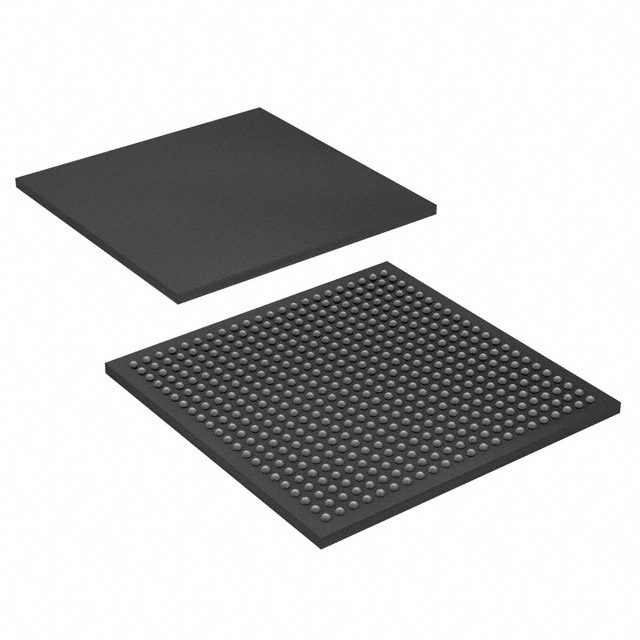
Package: The LCMXO3LF-9400C-5BG484I comes in a 484-ball grid array (BGA) package, which provides a compact and reliable solution for mounting the device onto a printed circuit board (PCB).
Essence: The essence of the LCMXO3LF-9400C-5BG484I lies in its ability to provide customizable logic functions, allowing designers to implement complex digital circuits with ease.
Packaging/Quantity: The LCMXO3LF-9400C-5BG484I is typically sold individually or in small quantities, depending on the requirements of the customer.
Specifications
- Logic Cells: 9,400
- I/O Pins: 484
- Operating Voltage: 1.2V
- Operating Temperature Range: -40°C to 85°C
- Speed Grade: 5 (maximum frequency of operation)
Detailed Pin Configuration
The LCMXO3LF-9400C-5BG484I has a total of 484 pins, each serving a specific purpose in the device's operation. A detailed pin configuration diagram can be found in the product datasheet.
Functional Features
- High-speed performance
- Low power consumption
- In-system programmability
- Support for various I/O standards
- On-chip memory resources
- Flexible clocking options
Advantages and Disadvantages
Advantages: - Versatile and customizable logic functions - Compact form factor - Low power consumption - Wide operating temperature range - In-system programmability
Disadvantages: - Limited number of logic cells compared to larger PLDs - Higher cost per logic cell compared to larger PLDs - May require additional support components for complex designs
Working Principles
The LCMXO3LF-9400C-5BG484I operates based on the principles of digital logic. It consists of a matrix of configurable logic blocks (CLBs) that can be programmed to perform specific logic functions. These CLBs are interconnected through a network of programmable interconnects, allowing designers to create custom digital circuits.
Detailed Application Field Plans
The LCMXO3LF-9400C-5BG484I finds applications in various fields, including: 1. Industrial automation 2. Communications systems 3. Consumer electronics 4. Automotive electronics 5. Medical devices
In industrial automation, it can be used for control systems and data processing. In communications systems, it can be utilized for signal processing and protocol implementation. In consumer electronics, it can enable advanced features in devices such as smartphones and gaming consoles. In automotive electronics, it can contribute to safety systems and vehicle control. In medical devices, it can assist in data acquisition and analysis.
Detailed and Complete Alternative Models
Some alternative models to the LCMXO3LF-9400C-5BG484I include: 1. LCMXO2LF-6400C-4BG256I 2. LCMXO3LF-6900C-6BG400I 3. LCMXO4LF-9000C-7BG484I 4. LCMXO5LF-1080E-8BG484I
These models offer different specifications and capabilities, allowing designers to choose the most suitable PLD for their specific requirements.
Word count: 511 words
10個與LCMXO3LF-9400C-5BG484I在技術方案中應用相關的常見問題與解答
Sure! Here are 10 common questions and answers related to the application of LCMXO3LF-9400C-5BG484I in technical solutions:
Q: What is the LCMXO3LF-9400C-5BG484I? A: The LCMXO3LF-9400C-5BG484I is a specific model of Field-Programmable Gate Array (FPGA) manufactured by Lattice Semiconductor.
Q: What is an FPGA? A: An FPGA is a type of integrated circuit that can be programmed after manufacturing, allowing for flexible hardware design and customization.
Q: What are the key features of the LCMXO3LF-9400C-5BG484I? A: Some key features include low power consumption, small form factor, high logic density, and support for various I/O standards.
Q: What are some typical applications of the LCMXO3LF-9400C-5BG484I? A: It can be used in a wide range of applications such as industrial automation, consumer electronics, telecommunications, automotive systems, and more.
Q: How can I program the LCMXO3LF-9400C-5BG484I? A: You can program the FPGA using Hardware Description Languages (HDLs) like VHDL or Verilog, along with specialized software tools provided by Lattice Semiconductor.
Q: Can I reprogram the LCMXO3LF-9400C-5BG484I multiple times? A: Yes, FPGAs are designed to be reprogrammable, allowing you to modify the functionality of the device as needed.
Q: What is the power supply requirement for the LCMXO3LF-9400C-5BG484I? A: The power supply voltage for this FPGA is typically 1.2V, but it can operate within a range of 1.14V to 1.26V.
Q: Does the LCMXO3LF-9400C-5BG484I support different I/O standards? A: Yes, it supports various I/O standards such as LVCMOS, LVTTL, LVDS, and SSTL, making it compatible with different interface requirements.
Q: Can I use the LCMXO3LF-9400C-5BG484I in high-speed applications? A: Yes, this FPGA has features like dedicated clock management resources and high-speed I/O capabilities, making it suitable for high-speed designs.
Q: Where can I find technical documentation and support for the LCMXO3LF-9400C-5BG484I? A: You can find technical documentation, datasheets, application notes, and support resources on the official website of Lattice Semiconductor or by contacting their customer support team.
Please note that the specific details and answers may vary depending on the manufacturer's specifications and guidelines.