

LCMXO2-640HC-6SG48I
Product Overview
Category
The LCMXO2-640HC-6SG48I belongs to the category of Field-Programmable Gate Arrays (FPGAs).
Use
FPGAs are integrated circuits that can be programmed or reprogrammed after manufacturing. The LCMXO2-640HC-6SG48I is specifically designed for use in various electronic applications that require programmable logic.
Characteristics
- High capacity: The LCMXO2-640HC-6SG48I offers a large number of logic cells, making it suitable for complex designs.
- Low power consumption: This FPGA is designed to operate efficiently with minimal power consumption.
- Small form factor: The package size and pin configuration allow for easy integration into compact electronic devices.
- High-speed performance: The LCMXO2-640HC-6SG48I offers fast processing capabilities, enabling rapid execution of complex algorithms.
Package
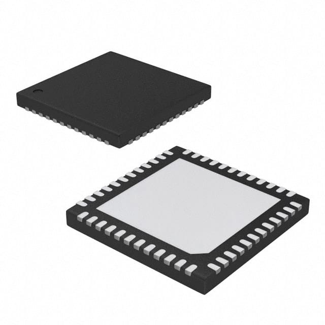
The LCMXO2-640HC-6SG48I comes in a 48-pin small-grid array (SGA) package.
Essence
The essence of the LCMXO2-640HC-6SG48I lies in its ability to provide flexible and customizable logic functions for electronic systems. It allows designers to implement their desired functionality by programming the FPGA.
Packaging/Quantity
The LCMXO2-640HC-6SG48I is typically sold individually or in reels containing multiple units, depending on the supplier. The exact quantity may vary.
Specifications
- Logic Cells: 640
- Maximum Frequency: 100 MHz
- Operating Voltage: 1.2V
- I/O Pins: 48
- Programmable Logic Blocks: 64
- Embedded Memory: 4.5 Kb
- Configuration Memory: 64 Kb
Detailed Pin Configuration
The LCMXO2-640HC-6SG48I has a total of 48 pins, each serving a specific purpose. The pin configuration is as follows:
(Pin Number) - (Pin Name) - (Function) 1 - VCCIO0 - I/O Power Supply 2 - GND - Ground 3 - IO0 - General Purpose I/O 4 - IO1 - General Purpose I/O 5 - IO2 - General Purpose I/O ... 48 - IO47 - General Purpose I/O
Functional Features
- Programmability: The LCMXO2-640HC-6SG48I can be programmed to implement various logic functions, allowing for customization and adaptability.
- Reconfigurability: The FPGA can be reprogrammed multiple times, enabling design changes or updates without the need for hardware modifications.
- I/O Flexibility: The device offers a sufficient number of I/O pins, allowing for easy interfacing with other electronic components.
- Low Power Consumption: The LCMXO2-640HC-6SG48I is designed to operate efficiently, minimizing power consumption in electronic systems.
Advantages and Disadvantages
Advantages
- High capacity and performance for complex designs
- Flexible and customizable logic functions
- Reconfigurable for design changes
- Small form factor for easy integration
- Low power consumption
Disadvantages
- Limited I/O pins compared to larger FPGAs
- Higher cost compared to fixed-function integrated circuits
Working Principles
The LCMXO2-640HC-6SG48I operates based on the principles of digital logic. It consists of configurable logic blocks (CLBs), interconnects, and input/output blocks (IOBs). The CLBs contain look-up tables (LUTs) that can be programmed to implement desired logic functions. The interconnects provide routing paths between the CLBs and IOBs, enabling data flow. The IOBs facilitate communication with external devices through the I/O pins.
Detailed Application Field Plans
The LCMXO2-640HC-6SG48I finds applications in various fields, including:
- Embedded Systems: It can be used in embedded systems for controlling and interfacing with peripherals.
- Communications: The FPGA can be employed in communication systems for signal processing and protocol implementation.
- Industrial Automation: It enables the implementation of custom control algorithms in industrial automation systems.
- Medical Devices: The LCMXO2-640HC-6SG48I can be utilized in medical devices for data acquisition and processing.
- Automotive Electronics: It finds application in automotive electronics for implementing advanced driver assistance systems (ADAS) and infotainment systems.
Detailed and Complete Alternative Models
- LCMXO2-1200HC-4TG144C
- LCMXO2-2000HC-4BG256C
- LCM
10個與LCMXO2-640HC-6SG48I在技術方案中應用相關的常見問題與解答
Sure! Here are 10 common questions and answers related to the application of LCMXO2-640HC-6SG48I in technical solutions:
Q: What is the LCMXO2-640HC-6SG48I? A: The LCMXO2-640HC-6SG48I is a low-cost, low-power FPGA (Field-Programmable Gate Array) device manufactured by Lattice Semiconductor.
Q: What are the key features of the LCMXO2-640HC-6SG48I? A: Some key features include 640 LUTs (Look-Up Tables), 64 I/O pins, 8Kbits of embedded memory, and support for various I/O standards.
Q: What are some typical applications of the LCMXO2-640HC-6SG48I? A: The LCMXO2-640HC-6SG48I is commonly used in applications such as industrial control systems, consumer electronics, communication devices, and automotive systems.
Q: How can I program the LCMXO2-640HC-6SG48I? A: The LCMXO2-640HC-6SG48I can be programmed using Lattice's proprietary design software called "Lattice Diamond" or other compatible programming tools.
Q: What voltage levels does the LCMXO2-640HC-6SG48I support? A: The LCMXO2-640HC-6SG48I supports both 3.3V and 1.2V voltage levels, making it compatible with a wide range of digital systems.
Q: Can I use the LCMXO2-640HC-6SG48I in battery-powered devices? A: Yes, the LCMXO2-640HC-6SG48I is designed to be low-power and can be used in battery-powered devices where power efficiency is crucial.
Q: Can I interface the LCMXO2-640HC-6SG48I with other components or microcontrollers? A: Yes, the LCMXO2-640HC-6SG48I has multiple I/O pins that can be used to interface with other components or microcontrollers using various communication protocols.
Q: Is the LCMXO2-640HC-6SG48I suitable for high-speed applications? A: While the LCMXO2-640HC-6SG48I is not specifically designed for high-speed applications, it can still handle moderate data rates depending on the specific requirements.
Q: Are there any development boards available for the LCMXO2-640HC-6SG48I? A: Yes, Lattice Semiconductor offers development boards like the "LCMXO2-640HC-6SG48I Breakout Board" that provide an easy way to prototype and test designs.
Q: Where can I find more information about the LCMXO2-640HC-6SG48I? A: You can find detailed technical documentation, datasheets, and application notes on Lattice Semiconductor's official website or by contacting their support team.