

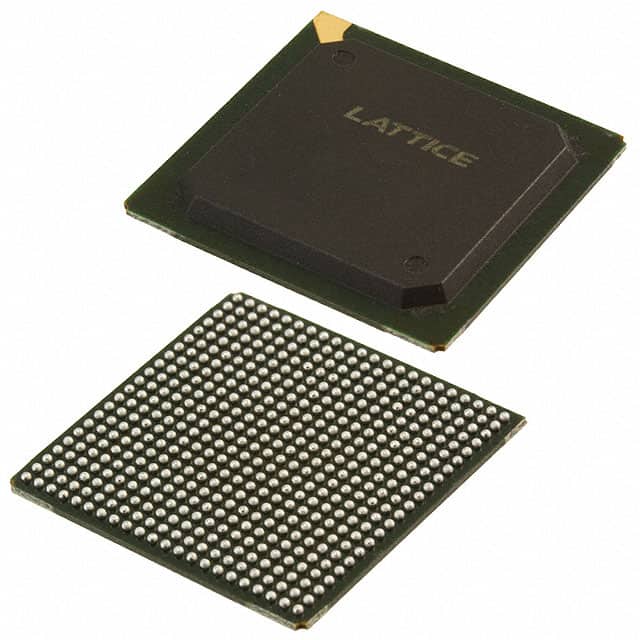
LCMXO2-4000HE-4FG484C
Product Overview
Category
The LCMXO2-4000HE-4FG484C belongs to the category of Field-Programmable Gate Arrays (FPGAs).
Use
FPGAs are integrated circuits that can be programmed and reprogrammed to perform various digital functions. The LCMXO2-4000HE-4FG484C is specifically designed for applications requiring high-performance and low-power consumption.
Characteristics
- High performance: The LCMXO2-4000HE-4FG484C offers a large number of logic elements and built-in memory blocks, enabling complex digital designs.
- Low power consumption: This FPGA is optimized for power efficiency, making it suitable for battery-powered devices or energy-conscious applications.
- Small package size: The 4FG484C package ensures a compact footprint, allowing for space-efficient designs.
- Robustness: The LCMXO2-4000HE-4FG484C is designed to withstand harsh environmental conditions, making it suitable for industrial applications.
Package and Quantity
The LCMXO2-4000HE-4FG484C is available in a 484-pin Fine-Pitch Ball Grid Array (FBGA) package. It is typically sold individually or in small quantities.
Specifications
- Logic Elements: 4,000
- Look-Up Tables (LUTs): 3,200
- Flip-Flops: 8,000
- Block RAM: 112 Kbits
- Maximum Operating Frequency: 300 MHz
- I/O Pins: 317
- Voltage Range: 1.14V - 1.26V
- Operating Temperature Range: -40°C to 100°C
Detailed Pin Configuration
The LCMXO2-4000HE-4FG484C has a total of 484 pins, each serving a specific purpose. The pin configuration includes dedicated input/output pins, power supply pins, ground pins, and configuration pins. A detailed pinout diagram can be found in the product datasheet.
Functional Features
The LCMXO2-4000HE-4FG484C offers several functional features that enhance its versatility and performance:
- Programmability: The FPGA can be programmed using Hardware Description Languages (HDLs) such as VHDL or Verilog, allowing for flexible and customizable digital designs.
- Embedded Memory: The built-in memory blocks enable efficient storage and retrieval of data, enhancing the overall performance of the FPGA.
- I/O Flexibility: The FPGA provides a wide range of I/O options, including differential signaling, LVDS, and single-ended interfaces, enabling seamless integration with external devices.
- Clock Management: The device incorporates clock management resources, such as phase-locked loops (PLLs), to generate and distribute precise clock signals throughout the design.
- Design Security: The LCMXO2-4000HE-4FG484C supports bitstream encryption and authentication, ensuring the integrity and confidentiality of the programmed design.
Advantages and Disadvantages
Advantages
- High-performance capabilities suitable for complex digital designs.
- Low power consumption, making it ideal for energy-efficient applications.
- Compact package size allows for space-saving designs.
- Robustness enables reliable operation in harsh environments.
- Versatile I/O options facilitate seamless integration with external devices.
Disadvantages
- Limited logic elements compared to higher-end FPGAs.
- Relatively smaller block RAM capacity may restrict certain memory-intensive applications.
- Higher cost compared to other programmable logic devices.
Working Principles
The LCMXO2-4000HE-4FG484C operates based on the principles of reconfigurable logic. It consists of an array of configurable logic blocks interconnected through programmable routing resources. The device can be programmed to implement various digital functions by configuring the interconnections and functionality of these logic blocks.
Detailed Application Field Plans
The LCMXO2-4000HE-4FG484C finds applications in a wide range of fields, including:
- Communications: Used in wireless base stations, network routers, and data communication equipment.
- Industrial Control: Employed in automation systems, motor control, and robotics.
- Consumer Electronics: Integrated into smart home devices, wearable technology, and multimedia systems.
- Automotive: Utilized in automotive infotainment systems, driver assistance, and engine control units.
- Aerospace and Defense: Applied in avionics, radar systems, and military communication equipment.
Alternative Models
For those seeking alternative options, the following FPGAs can be considered:
- Xilinx Spartan-6 XC6SLX9
- Intel Cyclone IV EP4CE6E22C8N
- Microsemi IGLOO2 M2GL090
10個與LCMXO2-4000HE-4FG484C在技術方案中應用相關的常見問題與解答
Sure! Here are 10 common questions and answers related to the application of LCMXO2-4000HE-4FG484C in technical solutions:
Q: What is the LCMXO2-4000HE-4FG484C? A: The LCMXO2-4000HE-4FG484C is a low-cost, low-power FPGA (Field-Programmable Gate Array) device manufactured by Lattice Semiconductor.
Q: What are the key features of the LCMXO2-4000HE-4FG484C? A: Some key features include 4000 Look-Up Tables (LUTs), 128 Kbits of embedded block RAM, 34 user I/O pins, and support for various I/O standards.
Q: What are some typical applications of the LCMXO2-4000HE-4FG484C? A: The LCMXO2-4000HE-4FG484C is commonly used in applications such as industrial control systems, consumer electronics, communication devices, and automotive systems.
Q: How can I program the LCMXO2-4000HE-4FG484C? A: The LCMXO2-4000HE-4FG484C can be programmed using Lattice Diamond or Lattice Radiant software tools, which provide a graphical interface for designing and programming the FPGA.
Q: What voltage levels does the LCMXO2-4000HE-4FG484C support? A: The LCMXO2-4000HE-4FG484C supports both 3.3V and 1.2V voltage levels, allowing for compatibility with a wide range of external devices.
Q: Can I use the LCMXO2-4000HE-4FG484C in battery-powered applications? A: Yes, the LCMXO2-4000HE-4FG484C is designed to be low-power and can be used in battery-powered applications where power consumption is a concern.
Q: Does the LCMXO2-4000HE-4FG484C support any communication protocols? A: Yes, the LCMXO2-4000HE-4FG484C supports various communication protocols such as SPI, I2C, UART, and GPIO, making it versatile for interfacing with other devices.
Q: Can I reprogram the LCMXO2-4000HE-4FG484C multiple times? A: Yes, the LCMXO2-4000HE-4FG484C is a reprogrammable FPGA, allowing you to modify and reconfigure its functionality multiple times during development or in the field.
Q: Are there any development boards available for the LCMXO2-4000HE-4FG484C? A: Yes, Lattice Semiconductor provides development boards like the LCMXO2-4000HE-B-EVN, which are specifically designed for prototyping and evaluating the LCMXO2-4000HE-4FG484C.
Q: Where can I find more technical documentation and resources for the LCMXO2-4000HE-4FG484C? A: You can find more technical documentation, datasheets, application notes, and reference designs on the official Lattice Semiconductor website or by contacting their support team.
Please note that the answers provided here are general and may vary depending on specific requirements and use cases. It's always recommended to refer to the official documentation and consult with experts for detailed information.