

LCMXO2-4000HC-5QN84C
Product Overview
Category
The LCMXO2-4000HC-5QN84C belongs to the category of Field-Programmable Gate Arrays (FPGAs).
Use
FPGAs are integrated circuits that can be programmed and reprogrammed to perform various digital functions. The LCMXO2-4000HC-5QN84C is specifically designed for applications requiring high-performance and low-power consumption.
Characteristics
- High performance: The LCMXO2-4000HC-5QN84C offers a high logic density and fast processing capabilities, making it suitable for complex digital designs.
- Low power consumption: This FPGA is designed to minimize power consumption, making it ideal for battery-powered devices or energy-efficient applications.
- Small package size: The LCMXO2-4000HC-5QN84C comes in a compact package, allowing for space-saving integration into electronic systems.
- Versatile I/O options: It provides a wide range of input/output options, enabling connectivity with other components and peripherals.
- Robust packaging: The LCMXO2-4000HC-5QN84C is available in a quality package that ensures protection against environmental factors and mechanical stress.
Packaging/Quantity
The LCMXO2-4000HC-5QN84C is typically packaged in trays or reels, depending on the manufacturer's specifications. The quantity per package may vary, but it is commonly available in quantities of 100 or more.
Specifications
- Logic Cells: 4,000
- Look-Up Tables (LUTs): 2,688
- Flip-Flops: 5,376
- Block RAM: 112 Kbits
- Maximum Frequency: 200 MHz
- Operating Voltage: 1.2V
- I/O Voltage: 3.3V
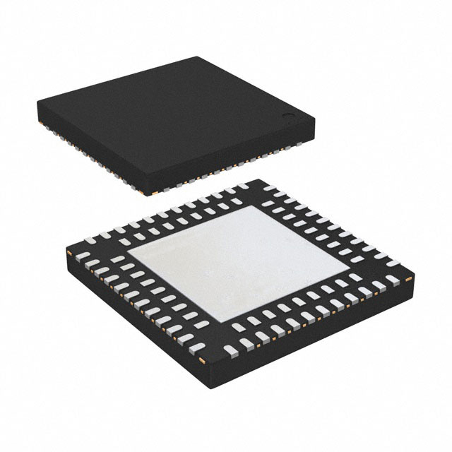
- Package Type: QFN (Quad Flat No-Lead)
- Package Size: 8mm x 8mm
- Temperature Range: -40°C to +85°C
Detailed Pin Configuration
The LCMXO2-4000HC-5QN84C has a total of 84 pins, which are assigned for various functions such as input, output, power supply, and configuration. The pin configuration may vary depending on the specific application requirements. Refer to the manufacturer's datasheet for the detailed pinout diagram.
Functional Features
- Programmability: The LCMXO2-4000HC-5QN84C can be programmed using Hardware Description Languages (HDL) or graphical design tools, allowing for flexible customization.
- Reconfigurability: It supports dynamic reconfiguration, enabling changes to the FPGA's functionality without requiring hardware modifications.
- Embedded Memory: The built-in Block RAM provides dedicated memory resources for data storage and retrieval, enhancing performance in memory-intensive applications.
- Clock Management: The FPGA includes clock management features, such as Phase-Locked Loops (PLLs), to generate and distribute clock signals accurately.
- I/O Flexibility: The LCMXO2-4000HC-5QN84C offers a wide range of I/O standards and voltage levels, facilitating seamless integration with other components and interfaces.
Advantages and Disadvantages
Advantages
- High-performance capabilities suitable for complex digital designs.
- Low power consumption, making it ideal for energy-efficient applications.
- Compact package size allows for space-saving integration.
- Versatile I/O options enable connectivity with various peripherals.
- Robust packaging ensures protection against environmental factors and mechanical stress.
Disadvantages
- Limited logic cell count compared to higher-end FPGAs.
- May require additional external components for certain applications.
- Higher cost compared to other programmable logic devices.
Working Principles
The LCMXO2-4000HC-5QN84C operates based on the principles of reconfigurable computing. It consists of an array of configurable logic blocks interconnected through programmable routing resources. The FPGA's functionality is determined by the configuration data stored in its internal memory. During operation, the FPGA executes the programmed logic functions and routes signals between different blocks to perform the desired digital processing tasks.
Detailed Application Field Plans
The LCMXO2-4000HC-5QN84C finds applications in various fields, including but not limited to: - Embedded systems - Digital signal processing - Communications - Industrial automation - Robotics - Internet of Things (IoT) - Medical devices - Automotive electronics
In embedded systems, it can be used for real-time control, sensor interfacing, and data processing. In digital signal processing, the FPGA enables high-speed computations and algorithm acceleration. In communications, it facilitates protocol handling, encryption/decryption, and network packet processing. The LCMXO2-4000HC-
10個與LCMXO2-4000HC-5QN84C在技術方案中應用相關的常見問題與解答
Sure! Here are 10 common questions and answers related to the application of LCMXO2-4000HC-5QN84C in technical solutions:
Q: What is the LCMXO2-4000HC-5QN84C? A: The LCMXO2-4000HC-5QN84C is a low-cost, low-power FPGA (Field-Programmable Gate Array) device manufactured by Lattice Semiconductor.
Q: What are the key features of the LCMXO2-4000HC-5QN84C? A: Some key features include 4000 Look-Up Tables (LUTs), 64 I/O pins, 4-input look-up table (LUT) with programmable flip-flop, and low power consumption.
Q: What are some typical applications of the LCMXO2-4000HC-5QN84C? A: The LCMXO2-4000HC-5QN84C is commonly used in applications such as industrial control systems, consumer electronics, communication devices, and automotive systems.
Q: How can I program the LCMXO2-4000HC-5QN84C? A: The LCMXO2-4000HC-5QN84C can be programmed using Lattice Diamond or Lattice Radiant software tools provided by Lattice Semiconductor.
Q: What is the maximum operating frequency of the LCMXO2-4000HC-5QN84C? A: The maximum operating frequency of the LCMXO2-4000HC-5QN84C depends on the design and implementation, but it can typically reach frequencies up to 200 MHz.
Q: Can I use the LCMXO2-4000HC-5QN84C for high-speed data processing? A: Yes, the LCMXO2-4000HC-5QN84C can be used for high-speed data processing due to its low propagation delay and efficient logic utilization.
Q: Does the LCMXO2-4000HC-5QN84C support external memory interfaces? A: Yes, the LCMXO2-4000HC-5QN84C supports various external memory interfaces such as SPI, I2C, UART, and DDR3.
Q: Can I use the LCMXO2-4000HC-5QN84C in battery-powered devices? A: Yes, the LCMXO2-4000HC-5QN84C is designed to be power-efficient, making it suitable for battery-powered devices that require FPGA functionality.
Q: What are the voltage requirements for the LCMXO2-4000HC-5QN84C? A: The LCMXO2-4000HC-5QN84C operates at a voltage range of 1.14V to 3.465V, making it compatible with various power supply configurations.
Q: Are there any development boards available for the LCMXO2-4000HC-5QN84C? A: Yes, Lattice Semiconductor provides development boards like the LCMXO2-4000HC-5UMG64C Breakout Board, which allows easy prototyping and evaluation of the FPGA.
Please note that the answers provided here are general and may vary depending on specific design requirements and application scenarios.