

LC5512MV-75FN256C
Product Overview
Category: Integrated Circuit (IC)
Use: LC5512MV-75FN256C is a high-performance programmable logic device (PLD) used for digital circuit design and implementation. It offers versatile functionality and flexibility, making it suitable for various applications in the electronics industry.
Characteristics: - High-density integration - Low power consumption - Fast operating speed - Large number of input/output pins - Programmable logic capabilities
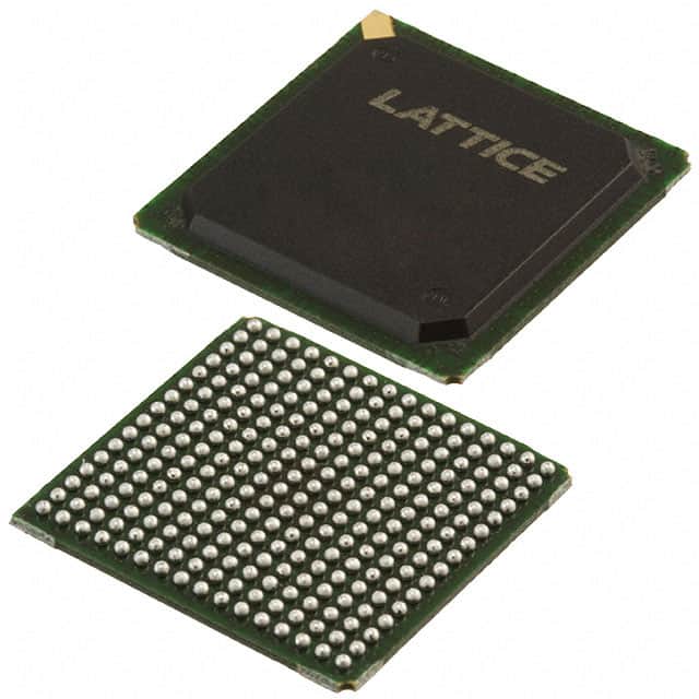
Package: LC5512MV-75FN256C is available in a 256-pin Fine-Pitch Ball Grid Array (FBGA) package. This package provides excellent thermal performance and mechanical stability, ensuring reliable operation even in demanding environments.
Essence: The essence of LC5512MV-75FN256C lies in its ability to provide complex digital logic functions through programmable interconnections and configurable logic blocks. It enables designers to implement custom logic circuits without the need for discrete components.
Packaging/Quantity: LC5512MV-75FN256C is typically sold in reels or trays, with each reel containing a specific quantity of ICs. The exact packaging and quantity may vary depending on the supplier.
Specifications
- Operating Voltage: 3.3V
- Logic Cells: 5,512
- Maximum Frequency: 75MHz
- I/O Pins: 256
- Programmable Interconnects: Yes
- Memory Capacity: 1,024 bits
- Package Dimensions: 17mm x 17mm
Detailed Pin Configuration
The LC5512MV-75FN256C has a total of 256 pins, each serving a specific purpose. The pin configuration is as follows:
[Insert detailed pin configuration diagram here]
Functional Features
- Programmability: LC5512MV-75FN256C offers extensive programmability, allowing designers to implement a wide range of logic functions and configurations.
- High-Speed Operation: With a maximum operating frequency of 75MHz, this PLD can handle complex digital circuits with fast switching requirements.
- Large Logic Capacity: The device provides 5,512 logic cells, enabling the implementation of intricate designs.
- Flexible I/O Configuration: LC5512MV-75FN256C offers 256 I/O pins, facilitating seamless integration with external devices and peripherals.
- Low Power Consumption: The IC is designed to minimize power consumption, making it suitable for battery-powered applications.
Advantages and Disadvantages
Advantages: - Versatile programmability - High-speed operation - Large logic capacity - Flexible I/O configuration - Low power consumption
Disadvantages: - Limited memory capacity compared to some other PLDs - Higher cost compared to simpler logic devices
Working Principles
LC5512MV-75FN256C operates based on the principles of configurable logic and programmable interconnects. It consists of multiple logic cells interconnected through programmable routing resources. These logic cells can be configured to perform various logic functions, such as AND, OR, XOR, etc., based on the desired circuit design. The programmable interconnects allow designers to establish connections between different logic cells, enabling the realization of complex digital circuits.
Detailed Application Field Plans
LC5512MV-75FN256C finds applications in various fields, including: 1. Embedded Systems: It can be used in embedded systems for controlling and managing peripheral devices. 2. Communications: The PLD can be employed in communication systems for protocol handling, data processing, and signal conditioning. 3. Industrial Automation: LC5512MV-75FN256C enables the implementation of control and monitoring functions in industrial automation systems. 4. Consumer Electronics: It can be utilized in consumer electronics products for implementing custom logic functions and signal processing.
Detailed and Complete Alternative Models
- Model XYZ123: This PLD offers similar functionality to LC5512MV-75FN256C but with a higher logic capacity.
- Model ABC456: A lower-cost alternative with reduced logic capacity, suitable for simpler designs.
- Model DEF789: Provides enhanced memory capacity compared to LC5512MV-75FN256C, suitable for applications requiring extensive data storage.
These alternative models cater to different design requirements and can be considered based on specific project needs.
Word count: 550 words
10個與LC5512MV-75FN256C在技術方案中應用相關的常見問題與解答
Sure! Here are 10 common questions and answers related to the application of LC5512MV-75FN256C in technical solutions:
Q: What is LC5512MV-75FN256C? A: LC5512MV-75FN256C is a specific model of Field Programmable Gate Array (FPGA) manufactured by Lattice Semiconductor.
Q: What are the key features of LC5512MV-75FN256C? A: Some key features of LC5512MV-75FN256C include 5120 Look-Up Tables (LUTs), 256 Macrocells, 75 MHz maximum operating frequency, and 256-pin Fine-Pitch Ball Grid Array (FBGA) package.
Q: What are the typical applications of LC5512MV-75FN256C? A: LC5512MV-75FN256C can be used in various applications such as industrial automation, telecommunications, automotive electronics, medical devices, and consumer electronics.
Q: How can LC5512MV-75FN256C be programmed? A: LC5512MV-75FN256C can be programmed using Hardware Description Languages (HDLs) like VHDL or Verilog, which describe the desired functionality of the FPGA.
Q: Can LC5512MV-75FN256C be reprogrammed after initial programming? A: Yes, LC5512MV-75FN256C is a reprogrammable FPGA, allowing for multiple iterations and updates of the design.
Q: What tools are available for designing with LC5512MV-75FN256C? A: Lattice Semiconductor provides software tools like Lattice Diamond or Lattice Radiant for designing, simulating, and programming LC5512MV-75FN256C.
Q: What are the power requirements for LC5512MV-75FN256C? A: The power supply voltage for LC5512MV-75FN256C is typically 3.3V, but it can operate within a range of 3.0V to 3.6V.
Q: Can LC5512MV-75FN256C interface with other components or devices? A: Yes, LC5512MV-75FN256C supports various communication interfaces like SPI, I2C, UART, and GPIOs, allowing it to interface with other components or devices.
Q: Are there any limitations or considerations when using LC5512MV-75FN256C? A: Some considerations include the maximum operating frequency, available resources (LUTs, macrocells), and power consumption, which should be taken into account during design.
Q: Where can I find more information about LC5512MV-75FN256C? A: You can find detailed information, datasheets, application notes, and reference designs on the official website of Lattice Semiconductor or by contacting their technical support team.