

LC4256V-75FTN256AI
Product Overview
Category: Integrated Circuit (IC)
Use: The LC4256V-75FTN256AI is a programmable logic device (PLD) that belongs to the family of Complex Programmable Logic Devices (CPLDs). It is designed for use in various digital applications, including telecommunications, industrial control systems, consumer electronics, and automotive electronics.
Characteristics: - High-density programmable logic device - Low power consumption - Fast performance - Flexible design options - Wide range of I/O capabilities
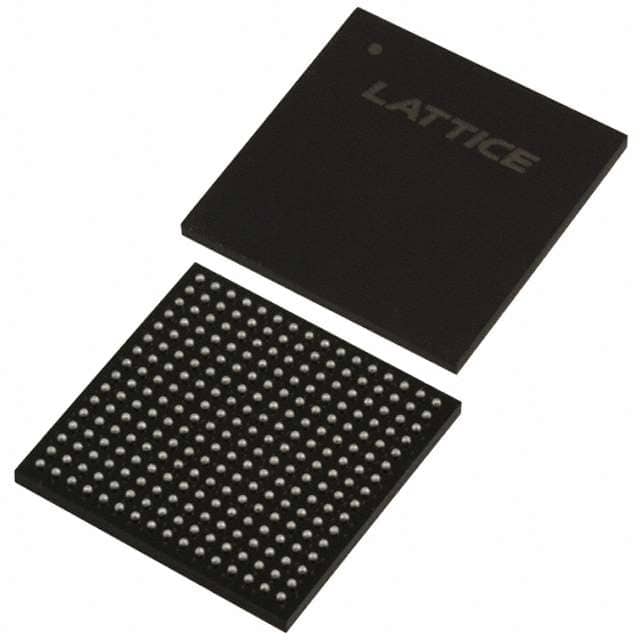
Package: The LC4256V-75FTN256AI is available in a 256-pin Fine-Pitch Ball Grid Array (FBGA) package. This package offers excellent thermal and electrical performance, ensuring reliable operation even in demanding environments.
Essence: The essence of the LC4256V-75FTN256AI lies in its ability to provide designers with a highly configurable and versatile solution for implementing complex digital logic functions. Its programmability allows for customization and adaptation to specific application requirements.
Packaging/Quantity: The LC4256V-75FTN256AI is typically sold in reels or trays, with a quantity of 250 units per reel/tray.
Specifications
- Logic Cells: 4,256
- Macrocells: 2,560
- Maximum User I/Os: 192
- Operating Voltage: 3.3V
- Speed Grade: -75
- Package Type: FBGA
- Package Pins: 256
- Temperature Range: -40°C to +85°C
Detailed Pin Configuration
The LC4256V-75FTN256AI has a total of 256 pins, each serving a specific purpose in the device's functionality. The pin configuration includes input/output pins, power supply pins, ground pins, and configuration pins. For a detailed pinout diagram and description, please refer to the manufacturer's datasheet.
Functional Features
- High-density programmable logic cells for complex digital designs
- Flexible I/O options for interfacing with external devices
- On-chip memory elements for data storage and processing
- Built-in clock management circuitry for precise timing control
- Support for various programming modes, including in-system programming (ISP)
- JTAG boundary scan for easy testing and debugging
Advantages and Disadvantages
Advantages: - High level of integration, reducing the need for additional components - Versatile and customizable design options - Low power consumption, suitable for battery-powered applications - Fast performance, enabling real-time processing - Wide temperature range for reliable operation in harsh environments
Disadvantages: - Limited number of user I/Os compared to some other PLD options - Higher cost compared to simpler logic devices - Steeper learning curve for inexperienced designers
Working Principles
The LC4256V-75FTN256AI operates based on the principles of programmable logic. It consists of an array of logic cells that can be interconnected and programmed to implement desired digital functions. The device is configured using a hardware description language (HDL) or a schematic entry tool, which defines the desired logic behavior. Once programmed, the device executes the specified logic operations, providing the desired functionality.
Detailed Application Field Plans
The LC4256V-75FTN256AI finds application in various fields, including:
- Telecommunications: Used in network switches, routers, and communication equipment for signal processing and protocol handling.
- Industrial Control Systems: Employed in automation systems, robotics, and process control applications for logic control and monitoring.
- Consumer Electronics: Integrated into audio/video equipment, gaming consoles, and home appliances for digital signal processing and control functions.
- Automotive Electronics: Utilized in automotive control units, infotainment systems, and driver assistance systems for implementing complex digital logic.
Detailed and Complete Alternative Models
- LC4128V-75TN100C: A lower-density CPLD with 1,280 logic cells and 100-pin TQFP package.
- LC4384V-75FTN256AI: A higher-density CPLD with 4,384 logic cells and 256-pin FBGA package.
- LC4032V-75TN48C: A compact CPLD with 3,200 logic cells and 48-pin TQFP package.
These alternative models offer different logic capacities, pin configurations, and package options to cater to various design requirements.
Word count: 537 words
10個與LC4256V-75FTN256AI在技術方案中應用相關的常見問題與解答
Sure! Here are 10 common questions and answers related to the application of LC4256V-75FTN256AI in technical solutions:
Q: What is LC4256V-75FTN256AI? A: LC4256V-75FTN256AI is a specific model of Field-Programmable Gate Array (FPGA) manufactured by Lattice Semiconductor.
Q: What are the key features of LC4256V-75FTN256AI? A: Some key features of LC4256V-75FTN256AI include 256 macrocells, 75MHz maximum operating frequency, and 5V tolerant I/O pins.
Q: In what applications can LC4256V-75FTN256AI be used? A: LC4256V-75FTN256AI can be used in various applications such as industrial automation, automotive electronics, telecommunications, and consumer electronics.
Q: How does LC4256V-75FTN256AI differ from other FPGAs? A: LC4256V-75FTN256AI offers a balance between cost, performance, and power consumption, making it suitable for many general-purpose applications.
Q: Can LC4256V-75FTN256AI be reprogrammed after deployment? A: Yes, LC4256V-75FTN256AI is a field-programmable device, meaning it can be reprogrammed even after it has been deployed in a system.
Q: What development tools are available for programming LC4256V-75FTN256AI? A: Lattice Semiconductor provides software tools like Lattice Diamond and iCEcube2 that support the programming and configuration of LC4256V-75FTN256AI.
Q: What are the power requirements for LC4256V-75FTN256AI? A: LC4256V-75FTN256AI typically operates at a voltage range of 3.3V, but it has 5V tolerant I/O pins, allowing compatibility with higher voltage systems.
Q: Can LC4256V-75FTN256AI interface with other components or devices? A: Yes, LC4256V-75FTN256AI can interface with various components and devices through its I/O pins, supporting protocols like SPI, I2C, UART, and more.
Q: Are there any limitations or considerations when using LC4256V-75FTN256AI? A: Some considerations include the maximum operating frequency, available macrocells, and the need for external memory if additional storage is required.
Q: Where can I find more information about LC4256V-75FTN256AI? A: You can find more detailed information about LC4256V-75FTN256AI in the datasheet provided by Lattice Semiconductor on their official website.