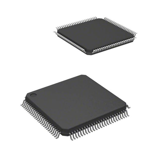
LC4064V-75TN100E
Product Overview
Category
LC4064V-75TN100E belongs to the category of Field Programmable Gate Arrays (FPGAs).
Use
This product is primarily used in digital logic circuits for various applications such as telecommunications, automotive electronics, consumer electronics, and industrial automation.
Characteristics
- LC4064V-75TN100E is a high-performance FPGA with 64 macrocells.
- It offers low power consumption and high-speed operation.
- The device operates at a voltage range of 3.3V.
- It supports various I/O standards, including LVCMOS, LVTTL, and SSTL.
Package
LC4064V-75TN100E comes in a Thin Quad Flat Pack (TQFP) package.
Essence
The essence of LC4064V-75TN100E lies in its ability to provide flexible and reconfigurable digital logic functionality, allowing designers to implement complex systems on a single chip.
Packaging/Quantity
LC4064V-75TN100E is typically packaged in reels or trays, with a quantity of 100 units per package.
Specifications
- Number of Macrocells: 64
- Operating Voltage: 3.3V
- Package Type: TQFP
- Maximum Frequency: 75 MHz
- I/O Standards: LVCMOS, LVTTL, SSTL
Detailed Pin Configuration
The pin configuration of LC4064V-75TN100E is as follows:
- VCCIO
- GND
- IO0
- IO1
- IO2
- IO3
- IO4
- IO5
- IO6
- IO7
- IO8
- IO9
- IO10
- IO11
- IO12
- IO13
- IO14
- IO15
- IO16
- IO17
- IO18
- IO19
- IO20
- IO21
- IO22
- IO23
- IO24
- IO25
- IO26
- IO27
- IO28
- IO29
- IO30
- IO31
- IO32
- IO33
- IO34
- IO35
- IO36
- IO37
- IO38
- IO39
- IO40
- IO41
- IO42
- IO43
- IO44
- IO45
- IO46
- IO47
- IO48
- IO49
- IO50
- IO51
- IO52
- IO53
- IO54
- IO55
- IO56
- IO57
- IO58
- IO59
- IO60
- IO61
- IO62
- IO63
- GND
- VCCIO
Functional Features
- LC4064V-75TN100E offers a wide range of programmable logic elements, including look-up tables (LUTs), flip-flops, and multiplexers.
- It supports various I/O standards, allowing easy interfacing with other digital components.
- The device provides on-chip memory resources for efficient data storage and retrieval.
- LC4064V-75TN100E supports advanced features like clock management, phase-locked loops (PLLs), and built-in self-test (BIST) capabilities.
Advantages and Disadvantages
Advantages
- High-performance FPGA with 64 macrocells.
- Low power consumption.
- Wide range of I/O standards supported.
- Flexible and reconfigurable digital logic functionality.
Disadvantages
- Limited number of macrocells compared to higher-end FPGAs.
- May require additional external components for certain applications.
Working Principles
LC4064V-75TN100E operates based on the principles of configurable logic. It consists of a matrix of programmable logic elements interconnected through configurable routing resources. The device can be programmed using hardware description languages (HDL) or graphical design tools, allowing designers to define the desired functionality of the circuit.
Detailed Application Field Plans
LC4064V-75TN100E finds applications in various fields, including:
- Telecommunications: Used in network routers, switches, and communication protocols.
- Automotive Electronics: Employed in automotive control systems, driver assistance systems, and infotainment systems.
- Consumer Electronics: Utilized in smart TVs, gaming consoles, and home automation devices.
- Industrial Automation: Applied in programm
10個與LC4064V-75TN100E在技術方案中應用相關的常見問題與解答
Sure! Here are 10 common questions and answers related to the application of LC4064V-75TN100E in technical solutions:
Q: What is LC4064V-75TN100E? A: LC4064V-75TN100E is a specific model of Field Programmable Gate Array (FPGA) manufactured by Lattice Semiconductor.
Q: What is an FPGA? A: FPGA stands for Field Programmable Gate Array, which is a type of integrated circuit that can be programmed after manufacturing to perform specific functions.
Q: What are the key features of LC4064V-75TN100E? A: Some key features of LC4064V-75TN100E include 64 macrocells, 64 I/O pins, 75MHz maximum operating frequency, and a TQFP-100 package.
Q: What are the typical applications of LC4064V-75TN100E? A: LC4064V-75TN100E is commonly used in various technical solutions such as industrial automation, robotics, telecommunications, automotive electronics, and medical devices.
Q: How can LC4064V-75TN100E be programmed? A: LC4064V-75TN100E can be programmed using Hardware Description Languages (HDLs) like VHDL or Verilog, which describe the desired functionality of the FPGA.
Q: Can LC4064V-75TN100E be reprogrammed? A: Yes, LC4064V-75TN100E is a reprogrammable FPGA, allowing users to modify its functionality by reprogramming it with new designs.
Q: What tools are required to program LC4064V-75TN100E? A: To program LC4064V-75TN100E, you will need a compatible development board or programmer, as well as the necessary software tools provided by Lattice Semiconductor.
Q: What is the power supply requirement for LC4064V-75TN100E? A: LC4064V-75TN100E typically operates at a voltage range of 3.3V, but it is recommended to consult the datasheet for detailed power supply specifications.
Q: Can LC4064V-75TN100E interface with other electronic components? A: Yes, LC4064V-75TN100E can interface with various electronic components such as sensors, actuators, memory devices, and communication modules through its I/O pins.
Q: Are there any limitations or considerations when using LC4064V-75TN100E? A: Some considerations include the limited number of macrocells and I/O pins, the maximum operating frequency, and the need for proper design and verification techniques to ensure correct functionality.
Please note that these answers are general and may vary depending on specific requirements and use cases.


