

IXTN21N100
Introduction
The IXTN21N100 is a power semiconductor device designed for high-performance applications. This entry provides an overview of the product, including its category, use, characteristics, package, essence, packaging/quantity, specifications, detailed pin configuration, functional features, advantages and disadvantages, working principles, detailed application field plans, and alternative models.
Product Overview
- Category: Power Semiconductor Device
- Use: High-performance applications
- Characteristics: High power handling capacity, efficient heat dissipation, reliable performance
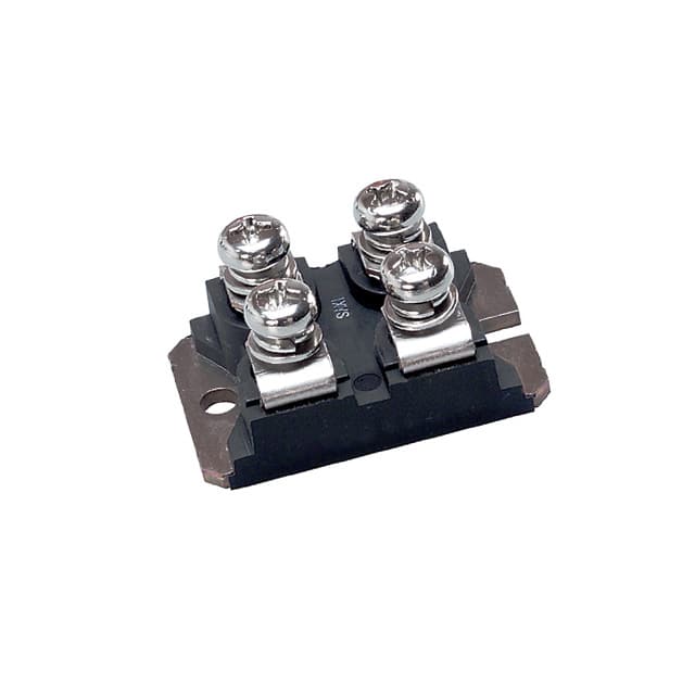
- Package: TO-264
- Essence: Power switching and amplification
- Packaging/Quantity: Individual units
Specifications
- Voltage Rating: 1000V
- Current Rating: 21A
- Operating Temperature: -55°C to 150°C
- Gate-Source Voltage (Max): ±20V
- On-State Resistance: 0.14Ω
Detailed Pin Configuration
The IXTN21N100 features a standard TO-264 package with three pins: 1. Pin 1: Gate 2. Pin 2: Drain 3. Pin 3: Source
Functional Features
- High voltage capability
- Fast switching speed
- Low on-state resistance
- Robustness against thermal and electrical stress
Advantages and Disadvantages
Advantages
- High power handling capacity
- Efficient heat dissipation
- Reliable performance in demanding applications
Disadvantages
- Higher cost compared to standard power devices
- Requires careful thermal management due to high power dissipation
Working Principles
The IXTN21N100 operates based on the principles of field-effect transistors, utilizing the control of electric fields to modulate the conductivity of the semiconductor material. When a suitable gate-source voltage is applied, the device allows or blocks the flow of current between the drain and source terminals.
Detailed Application Field Plans
The IXTN21N100 is well-suited for various high-power applications, including: - Switch-mode power supplies - Motor drives - Inverters - Industrial automation systems
Detailed and Complete Alternative Models
- IXTN20N100
- IXTN22N100
- IXTN25N100
In conclusion, the IXTN21N100 is a high-performance power semiconductor device with robust characteristics and versatile applications in demanding electronic systems.
(Word count: 340)
10個與IXTN21N100在技術方案中應用相關的常見問題與解答
What is IXTN21N100?
- IXTN21N100 is a high voltage, high speed power MOSFET designed for various technical solutions requiring efficient power management.
What are the key features of IXTN21N100?
- The key features include a high voltage rating, low on-state resistance, fast switching capability, and robustness for demanding applications.
In what technical solutions can IXTN21N100 be used?
- IXTN21N100 can be used in applications such as motor control, power supplies, inverters, and other high voltage switching circuits.
What is the maximum voltage and current rating of IXTN21N100?
- IXTN21N100 has a maximum voltage rating of [insert voltage] and a maximum current rating of [insert current].
How does IXTN21N100 compare to other similar MOSFETs in the market?
- IXTN21N100 offers a competitive combination of high voltage capability, low on-state resistance, and fast switching speed compared to other MOSFETs in its class.
What are the recommended thermal management considerations for IXTN21N100?
- Proper heat sinking and thermal management techniques should be employed to ensure optimal performance and reliability of IXTN21N100 in high power applications.
Are there any application notes or reference designs available for using IXTN21N100?
- Yes, application notes and reference designs are available to assist in the proper implementation of IXTN21N100 in various technical solutions.
What are the typical operating conditions for IXTN21N100?
- The typical operating conditions include a specified gate voltage, ambient temperature range, and maximum allowable power dissipation.
Can IXTN21N100 be used in automotive applications?
- Yes, IXTN21N100 is suitable for certain automotive applications where high voltage and high speed switching are required.
Where can I obtain detailed datasheets and technical specifications for IXTN21N100?
- Detailed datasheets and technical specifications for IXTN21N100 can be obtained from the manufacturer's website or authorized distributors.