

EPM570F100I5
Product Overview
Category
EPM570F100I5 belongs to the category of Field-Programmable Gate Arrays (FPGAs).
Use
This FPGA is designed for various applications that require high-performance digital signal processing, such as telecommunications, automotive, and industrial control systems.
Characteristics
- High-speed processing capabilities
- Configurable logic blocks
- On-chip memory resources
- Flexible I/O interfaces
- Low power consumption
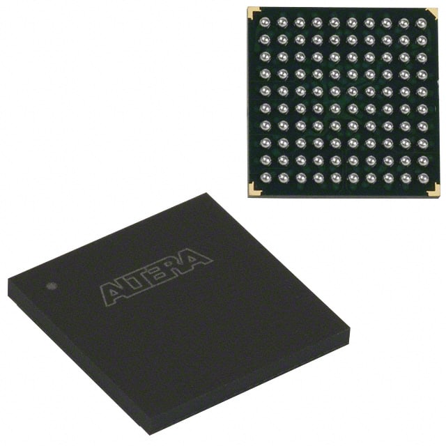
Package
EPM570F100I5 is available in a compact and durable package, ensuring easy integration into electronic systems. The package provides protection against environmental factors and facilitates efficient heat dissipation.
Essence
The essence of EPM570F100I5 lies in its ability to provide reconfigurable hardware that can be programmed to perform specific tasks, offering flexibility and adaptability in various applications.
Packaging/Quantity
Each EPM570F100I5 unit is packaged individually and comes with all necessary documentation and support materials. The quantity per package depends on the supplier and customer requirements.
Specifications
- Logic Elements: 570,000
- Embedded Memory: 1,638 Kbits
- Maximum User I/Os: 316
- Maximum User I/O Pins: 260
- Operating Voltage: 1.2V
- Operating Temperature Range: -40°C to 100°C
- Speed Grade: 5
Detailed Pin Configuration
The pin configuration of EPM570F100I5 is as follows:
| Pin Number | Pin Name | Description | |------------|----------|-------------| | 1 | VCCINT | Internal core voltage supply | | 2 | GND | Ground | | 3 | IOB0 | User I/O Bank 0 | | ... | ... | ... | | 316 | IOB315 | User I/O Bank 315 |
Functional Features
- High-speed data processing
- Configurable logic blocks for custom circuit implementation
- Dedicated DSP blocks for efficient signal processing
- On-chip memory resources for data storage and retrieval
- Flexible I/O interfaces for seamless integration with external devices
- Clock management resources for precise timing control
Advantages and Disadvantages
Advantages
- Versatile and adaptable to various applications
- High-performance processing capabilities
- Low power consumption compared to traditional ASICs
- Rapid prototyping and development cycles
- Cost-effective solution for complex digital systems
Disadvantages
- Steeper learning curve for programming and design
- Limited scalability compared to custom-designed ASICs
- Higher cost per unit compared to mass-produced integrated circuits
Working Principles
EPM570F100I5 operates based on the principles of reconfigurable hardware. It consists of an array of configurable logic blocks interconnected through programmable routing resources. The device can be programmed using Hardware Description Languages (HDL) such as VHDL or Verilog, allowing users to define the desired functionality of the FPGA.
Upon programming, the configuration data is stored in on-chip memory elements, enabling the FPGA to perform the specified tasks. The flexible I/O interfaces facilitate communication between the FPGA and external devices, while the clock management resources ensure precise timing synchronization.
Detailed Application Field Plans
EPM570F100I5 finds extensive application in various fields, including:
- Telecommunications: Used in base stations, network routers, and optical communication systems for high-speed data processing and protocol handling.
- Automotive: Employed in advanced driver assistance systems (ADAS), engine control units (ECUs), and infotainment systems for real-time data processing and control.
- Industrial Control Systems: Utilized in programmable logic controllers (PLCs), robotics, and automation systems for precise control and monitoring of industrial processes.
- Medical Devices: Integrated into medical imaging systems, patient monitoring devices, and laboratory equipment for data acquisition and processing.
- Aerospace and Defense: Applied in radar systems, avionics, and military communication systems for high-performance signal processing and encryption.
Detailed and Complete Alternative Models
- EPM240T100C5N: A smaller FPGA with 240,000 logic elements, suitable for applications with lower complexity and power requirements.
- EPM1270F256I5N: A higher-end FPGA with 1,270,000 logic elements, offering increased processing capabilities for demanding applications.
- EPM570T100C5N: A cost-effective alternative with 570,000 logic elements, ideal for budget-conscious projects without compromising performance.
These alternative models provide a range of options to suit different project requirements, allowing users to select the most appropriate FPGA for their specific needs.
In conclusion, EPM570F100I5 is a versatile FPGA that offers high-performance digital signal processing capabilities. With its configurable logic blocks, flexible
10個與EPM570F100I5在技術方案中應用相關的常見問題與解答
Sure! Here are 10 common questions and answers related to the application of EPM570F100I5 in technical solutions:
Q: What is EPM570F100I5? A: EPM570F100I5 is a field-programmable gate array (FPGA) manufactured by Intel.
Q: What are the key features of EPM570F100I5? A: Some key features include 570,000 logic elements, 100 MHz maximum operating frequency, and 5V input/output voltage.
Q: In what technical solutions can EPM570F100I5 be used? A: EPM570F100I5 can be used in various applications such as industrial automation, telecommunications, automotive systems, and medical devices.
Q: How does EPM570F100I5 differ from other FPGAs? A: EPM570F100I5 offers a balance between performance and cost, making it suitable for a wide range of applications.
Q: Can EPM570F100I5 be reprogrammed after deployment? A: Yes, EPM570F100I5 is a field-programmable device, meaning it can be reprogrammed even after it has been deployed in a system.
Q: What programming languages can be used with EPM570F100I5? A: EPM570F100I5 can be programmed using hardware description languages (HDLs) such as VHDL or Verilog.
Q: Are there any development tools available for EPM570F100I5? A: Yes, Intel provides Quartus Prime software, which is a comprehensive development environment for designing and programming FPGAs like EPM570F100I5.
Q: Can EPM570F100I5 interface with other components or devices? A: Yes, EPM570F100I5 supports various communication protocols such as SPI, I2C, UART, and Ethernet, allowing it to interface with other components or devices.
Q: What is the power consumption of EPM570F100I5? A: The power consumption of EPM570F100I5 depends on the specific design and usage scenario. It is recommended to refer to the datasheet for detailed power specifications.
Q: Where can I find additional resources or support for EPM570F100I5? A: Intel's website provides documentation, application notes, and a community forum where you can find additional resources and support for EPM570F100I5.