

EP4CE15M8I7N
Product Overview
- Category: Programmable Logic Device (PLD)
- Use: EP4CE15M8I7N is a PLD used for digital logic design and implementation.
- Characteristics:
- High-performance device with low power consumption
- Offers high-speed data processing capabilities
- Provides flexibility in designing complex digital circuits
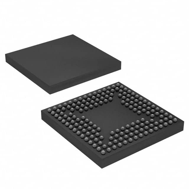
- Package: The EP4CE15M8I7N comes in a small form factor package, making it suitable for various applications.
- Essence: EP4CE15M8I7N is an essential component in the field of digital logic design, enabling the implementation of complex digital systems.
- Packaging/Quantity: The EP4CE15M8I7N is typically sold in reels or trays, with quantities varying based on customer requirements.
Specifications
- Logic Elements: 15,183
- Memory Bits: 608,256
- Maximum User I/O Pins: 179
- Operating Voltage: 1.2V
- Speed Grade: 8
- Package Type: FBGA
- Temperature Range: -40°C to +100°C
Detailed Pin Configuration
The EP4CE15M8I7N has a total of 179 user I/O pins, which can be configured as inputs or outputs based on the design requirements. These pins are distributed across the device and are labeled accordingly for easy identification and connection.
For a detailed pin configuration diagram, please refer to the official datasheet provided by the manufacturer.
Functional Features
- High-speed performance: The EP4CE15M8I7N offers fast data processing capabilities, making it suitable for applications requiring real-time operations.
- Flexibility: With its programmable nature, this PLD allows designers to implement a wide range of digital logic functions, providing flexibility in system design.
- Low power consumption: The device is designed to operate efficiently with low power consumption, making it suitable for battery-powered applications.
- Integrated memory: The EP4CE15M8I7N includes a significant amount of embedded memory, enabling the storage and retrieval of data within the device itself.
Advantages and Disadvantages
Advantages: - High-performance capabilities - Flexibility in design - Low power consumption - Integrated memory for efficient data handling
Disadvantages: - Limited number of user I/O pins - Requires expertise in digital logic design for optimal utilization
Working Principles
The EP4CE15M8I7N operates based on the principles of programmable logic. It consists of an array of configurable logic blocks (CLBs) interconnected through programmable interconnects. These CLBs can be programmed to implement various digital logic functions, such as combinational and sequential circuits.
The device is configured using a hardware description language (HDL), which allows designers to specify the desired functionality. Once programmed, the EP4CE15M8I7N executes the specified logic operations, enabling the desired digital system to function.
Detailed Application Field Plans
The EP4CE15M8I7N finds applications in various fields, including:
- Embedded Systems: Used in the development of embedded systems, where real-time processing and control are required.
- Communications: Employed in communication systems for signal processing, encryption, and protocol implementation.
- Industrial Automation: Utilized in industrial automation systems for controlling machinery, monitoring sensors, and data acquisition.
- Consumer Electronics: Integrated into consumer electronic devices for implementing complex functionalities, such as audio/video processing and user interfaces.
- Automotive: Applied in automotive electronics for functions like engine control, driver assistance systems, and infotainment.
Detailed and Complete Alternative Models
- EP4CE6E22C8N
- EP4CE10F17C8N
- EP4CE30F23C8N
- EP4CE40F29C8N
- EP4CE55F23C8N
These alternative models offer varying capacities and features, allowing designers to choose the most suitable PLD based on their specific requirements.
Note: The above information is subject to change. For the most accurate and up-to-date details, please refer to the official documentation provided by the manufacturer.
Word Count: 550
10個與EP4CE15M8I7N在技術方案中應用相關的常見問題與解答
Sure! Here are 10 common questions and answers related to the application of EP4CE15M8I7N in technical solutions:
Q: What is EP4CE15M8I7N? A: EP4CE15M8I7N is a field-programmable gate array (FPGA) chip manufactured by Intel (formerly Altera). It offers programmable logic, memory, and digital signal processing capabilities.
Q: What are the key features of EP4CE15M8I7N? A: Some key features include 15,408 logic elements, 270 embedded multipliers, 8 Mbits of RAM, and support for various I/O standards.
Q: How can EP4CE15M8I7N be used in technical solutions? A: EP4CE15M8I7N can be used in a wide range of applications such as industrial automation, telecommunications, automotive systems, medical devices, and more.
Q: Can EP4CE15M8I7N be programmed using a hardware description language (HDL)? A: Yes, EP4CE15M8I7N can be programmed using popular HDLs like VHDL or Verilog.
Q: What development tools are available for programming EP4CE15M8I7N? A: Intel Quartus Prime is the primary development tool used for designing, simulating, and programming EP4CE15M8I7N.
Q: Can EP4CE15M8I7N interface with other components or devices? A: Yes, EP4CE15M8I7N supports various communication protocols like UART, SPI, I2C, Ethernet, and PCIe, allowing it to interface with other components or devices.
Q: Can EP4CE15M8I7N be used for real-time signal processing? A: Yes, EP4CE15M8I7N's embedded multipliers and dedicated digital signal processing (DSP) blocks make it suitable for real-time signal processing applications.
Q: Is EP4CE15M8I7N suitable for low-power applications? A: EP4CE15M8I7N is not specifically designed for low-power applications, but power-saving techniques can be implemented to optimize its power consumption.
Q: Are there any limitations or considerations when using EP4CE15M8I7N? A: Some considerations include the available I/O pins, clock frequency limitations, and resource utilization constraints that need to be taken into account during design.
Q: Where can I find additional resources and support for EP4CE15M8I7N? A: Intel provides documentation, application notes, reference designs, and a community forum where users can find additional resources and support for EP4CE15M8I7N.
Please note that the specific details and answers may vary depending on the context and requirements of your technical solution.