

EP3C10E144I7N
Product Overview
- Category: Integrated Circuit (IC)
- Use: Programmable Logic Device (PLD)
- Characteristics: High-performance, low-power consumption
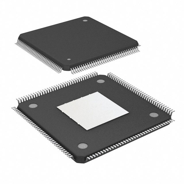
- Package: 144-pin Enhanced Plastic Quad Flat Pack (EPQFP)
- Essence: Versatile and flexible digital logic device
- Packaging/Quantity: Available in reels or trays, quantity varies based on supplier
Specifications
- Logic Elements: 10,080
- Embedded Memory: 414 kilobits
- Maximum User I/Os: 101
- Operating Voltage: 1.2V
- Operating Temperature: -40°C to 100°C
- Speed Grade: I7N
Detailed Pin Configuration
The EP3C10E144I7N has a total of 144 pins, each serving a specific purpose. The pin configuration is as follows:
- Pins 1-20: Ground (GND)
- Pins 21-28: Input/Output (I/O) pins
- Pins 29-36: Dedicated input pins
- Pins 37-44: Dedicated output pins
- Pins 45-48: Configuration pins
- Pins 49-56: Clock input pins
- Pins 57-64: Power supply (VCC)
- Pins 65-144: Reserved for various functions
Functional Features
- High-density programmable logic device
- Low power consumption for energy-efficient applications
- Supports various digital logic functions
- Flexible and reprogrammable design
- Offers embedded memory for data storage
- Provides clock management resources
- Supports multiple I/O standards
Advantages and Disadvantages
Advantages
- Versatile and adaptable for different applications
- High-performance capabilities
- Low power consumption for energy efficiency
- Compact size and high-density integration
- Reprogrammable design allows for flexibility
Disadvantages
- Limited number of I/O pins compared to larger PLDs
- Higher cost compared to simpler logic devices
- Requires specialized programming tools for configuration
Working Principles
The EP3C10E144I7N is based on programmable logic technology, utilizing a matrix of configurable logic elements (LEs) interconnected through programmable interconnect resources. The device can be programmed to implement various digital logic functions by configuring the LEs and interconnects using a hardware description language (HDL) or a graphical design tool.
Detailed Application Field Plans
The EP3C10E144I7N finds applications in various fields, including:
- Embedded Systems: Used for implementing control and interface functions in embedded systems.
- Communications: Utilized in networking equipment for data processing and protocol handling.
- Industrial Automation: Enables control and monitoring functions in industrial automation systems.
- Consumer Electronics: Integrated into consumer electronic devices for logic and interface functions.
- Automotive: Used in automotive electronics for control and communication purposes.
Alternative Models
For those seeking alternative options, the following models provide similar functionality:
- EP3C16E144I7N: Offers higher logic capacity with 16,128 logic elements.
- EP3C25E144I7N: Provides increased embedded memory capacity with 1,035 kilobits.
- EP3C40E144I7N: Offers a larger number of user I/Os with 161 pins.
These alternatives cater to different requirements and can be chosen based on specific project needs.
Word count: 330 words
10個與EP3C10E144I7N在技術方案中應用相關的常見問題與解答
Sure! Here are 10 common questions and answers related to the application of EP3C10E144I7N in technical solutions:
Q: What is EP3C10E144I7N? A: EP3C10E144I7N is a specific model of Field-Programmable Gate Array (FPGA) manufactured by Intel.
Q: What are the key features of EP3C10E144I7N? A: Some key features of EP3C10E144I7N include 10,080 logic elements, 414 user I/O pins, and support for various communication protocols.
Q: What are the typical applications of EP3C10E144I7N? A: EP3C10E144I7N is commonly used in applications such as industrial automation, robotics, telecommunications, and embedded systems.
Q: How can EP3C10E144I7N be programmed? A: EP3C10E144I7N can be programmed using hardware description languages (HDLs) like VHDL or Verilog, and programming tools provided by Intel.
Q: Can EP3C10E144I7N be reprogrammed after deployment? A: Yes, EP3C10E144I7N is a reprogrammable FPGA, allowing for flexibility and updates even after deployment.
Q: What are the power requirements for EP3C10E144I7N? A: EP3C10E144I7N typically operates at a voltage range of 1.15V to 1.25V, with additional power supply requirements for I/O banks and configuration pins.
Q: Does EP3C10E144I7N support external memory interfaces? A: Yes, EP3C10E144I7N supports various external memory interfaces like DDR2, DDR3, and QDR II+.
Q: Can EP3C10E144I7N interface with other devices or microcontrollers? A: Yes, EP3C10E144I7N can interface with other devices using protocols such as SPI, I2C, UART, and Ethernet.
Q: Are there any development boards available for EP3C10E144I7N? A: Yes, Intel provides development boards specifically designed for EP3C10E144I7N, which include necessary connectors and peripherals for prototyping.
Q: Where can I find documentation and support for EP3C10E144I7N? A: Documentation, datasheets, reference designs, and technical support for EP3C10E144I7N can be found on Intel's official website or community forums.
Please note that the answers provided here are general and may vary depending on specific requirements and use cases.