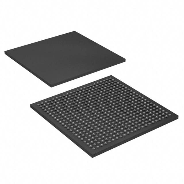
EP1S10F484I6
Product Overview
- Category: Programmable Logic Device (PLD)
- Use: EP1S10F484I6 is a PLD used for digital logic design and implementation.
- Characteristics:
- High-performance device with advanced features
- Flexible and reprogrammable
- Offers high-speed operation and low power consumption
- Package: The EP1S10F484I6 comes in a 484-pin FineLine BGA package.
- Essence: EP1S10F484I6 is designed to provide efficient and reliable programmable logic solutions.
- Packaging/Quantity: Each package contains one EP1S10F484I6 device.
Specifications
- Logic Elements: 10,000
- Maximum User I/Os: 346
- Embedded Memory: 288 Kbits
- Operating Voltage: 3.3V
- Speed Grade: 6
- Clock Networks: 4
- PLLs: 2
- Total RAM Bits: 18,432 bits
- Total DSP Blocks: 16
Detailed Pin Configuration
The EP1S10F484I6 has a total of 484 pins. The pin configuration is as follows:
- Pin 1: VCCIO
- Pin 2: GND
- Pin 3: TCK
- Pin 4: TMS
- Pin 5: TDI
- ...
- Pin 484: VCCINT
For the complete pin configuration, please refer to the product datasheet.
Functional Features
- High-performance programmable logic device
- Supports various digital logic functions
- Flexible and reprogrammable design
- Low power consumption
- High-speed operation
- Integrated memory and DSP blocks for enhanced functionality
Advantages and Disadvantages
Advantages: - High-performance and flexible design - Reprogrammable for easy modifications - Low power consumption - Integrated memory and DSP blocks enhance functionality
Disadvantages: - Limited logic elements compared to higher-end PLDs - Higher cost compared to simpler programmable logic devices
Working Principles
The EP1S10F484I6 operates based on the principles of programmable logic. It consists of a matrix of configurable logic elements that can be programmed to perform various digital logic functions. The device is configured using a hardware description language (HDL) and then programmed onto the PLD using specialized software tools. Once programmed, the EP1S10F484I6 can execute the desired logic operations.
Detailed Application Field Plans
The EP1S10F484I6 is widely used in various applications, including:
- Telecommunications: Used in network routers, switches, and communication equipment.
- Industrial Automation: Employed in control systems, PLCs, and robotics.
- Automotive: Utilized in automotive electronics, such as engine control units and infotainment systems.
- Consumer Electronics: Found in smart TVs, gaming consoles, and home automation systems.
- Medical Devices: Integrated into medical imaging equipment, patient monitoring systems, and diagnostic devices.
Detailed and Complete Alternative Models
- EP1S20F484C7: Similar to EP1S10F484I6 but with 20,000 logic elements.
- EP1S30F780I6: Higher-end model with 30,000 logic elements and advanced features.
- EP1S40F1020C6: Enhanced version with 40,000 logic elements and increased memory capacity.
These alternative models offer varying levels of performance and functionality, allowing users to choose the most suitable option for their specific requirements.
Note: The above information is subject to change. Please refer to the latest product documentation for accurate and up-to-date details.
Word Count: 511
10個與EP1S10F484I6在技術方案中應用相關的常見問題與解答
Sure! Here are 10 common questions and answers related to the application of EP1S10F484I6 in technical solutions:
Q1: What is EP1S10F484I6? A1: EP1S10F484I6 is a specific model of Field-Programmable Gate Array (FPGA) manufactured by Intel. It offers a range of programmable logic and I/O capabilities for various technical applications.
Q2: What are the key features of EP1S10F484I6? A2: EP1S10F484I6 features 10,000 logic elements, 484 pins, and supports various I/O standards such as LVDS, SSTL, and HSTL. It also includes embedded memory blocks and digital signal processing (DSP) blocks.
Q3: What are some typical applications of EP1S10F484I6? A3: EP1S10F484I6 can be used in a wide range of applications including industrial automation, telecommunications, automotive electronics, medical devices, and high-performance computing.
Q4: How can EP1S10F484I6 be programmed? A4: EP1S10F484I6 can be programmed using hardware description languages (HDLs) such as VHDL or Verilog. Intel provides development tools like Quartus Prime to facilitate programming and configuration.
Q5: Can EP1S10F484I6 interface with other components or devices? A5: Yes, EP1S10F484I6 supports various communication protocols such as SPI, I2C, UART, and Ethernet. It can interface with sensors, actuators, memory devices, and other peripherals.
Q6: What are the power requirements for EP1S10F484I6? A6: EP1S10F484I6 operates at a supply voltage of 1.2V and requires additional voltages for I/O banks, which can range from 1.5V to 3.3V depending on the specific requirements.
Q7: Can EP1S10F484I6 be reprogrammed after deployment? A7: Yes, EP1S10F484I6 is a reprogrammable FPGA, allowing for updates and modifications to the design even after it has been deployed in a system.
Q8: Are there any limitations or considerations when using EP1S10F484I6? A8: Some considerations include power consumption, thermal management, and timing constraints. It's important to carefully design and optimize the implementation to meet the desired performance goals.
Q9: Does Intel provide technical support for EP1S10F484I6? A9: Yes, Intel offers technical support through their website, forums, and documentation. They also provide application notes and reference designs to assist with the development process.
Q10: Where can I find more information about EP1S10F484I6? A10: You can find detailed information about EP1S10F484I6 on Intel's official website, including datasheets, user guides, and application notes specific to this FPGA model.
Please note that the answers provided here are general and may vary based on specific requirements and use cases.


